
1/2/2023 – 1/15/2023
Summary: Starting off the new year strong by grinding the textbook and wrapping up my backlog for sign orders from before the holidays. This year’s theme is Pokemon.
The designs are coming out without issues and the assembly process is getting faster and faster. I’m getting the hang of doing them quickly and error-free. Now that the last of the initial 12 signs are done, I’m pivoting to making the store page. I’m not really sweating the name or logo too much. Open to suggestions. Best name we’ve come up with so far is Neon Vision Custom Signs. Or just Neon Visions. Something like that.
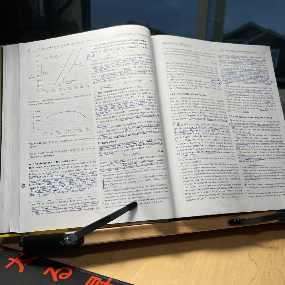
I’ve been reading Art of Electronics every day. At the very least turning the page once, to stay consistent. Rereading Chapter 2 and everything is starting to click into place. I’m understanding everything a lot more deeply with a second pass. I should be done with chapter 2 by the end of B and ready to move forward with Chapter 3 on FETs. I’m really hoping the book isn’t lying when it says chapters 1-3 are significantly harder. Either way, the goal is to know this book forwards and backwards by the end of the year. It’s not time wasted, because I’m having light bulb moments pretty much every time I look at the book now. There’s just a lot of information to take in and organize. The extended notes below are my reference notes that I’ve written such that I could teach this content to someone else. That’s a big reason why it’s taking so long. I’m not moving on from a section until I know how I could make it make sense for someone else.
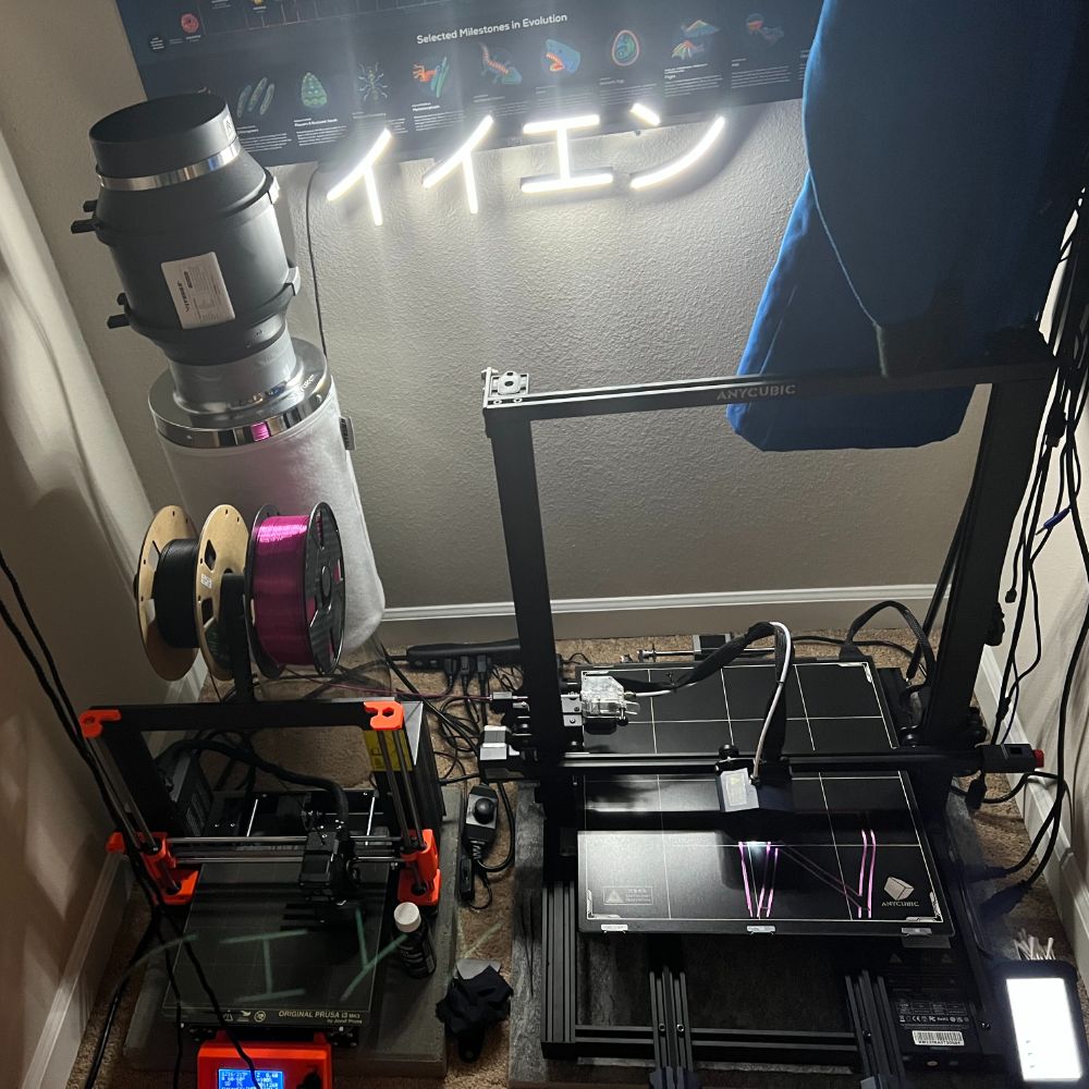
The primary focus for the lab right is is just grinding textbooks and setting up the signs as an income stream. Which isn’t very interesting from a dev log perspective, since I’m not prototyping or building too many new things. I have a feeling these posts will be a little dry for a while, unless you’re looking for electronics lessons or want to watch a small business shooting its shot.
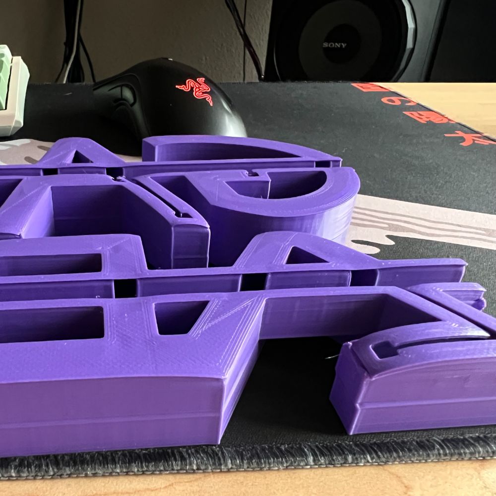
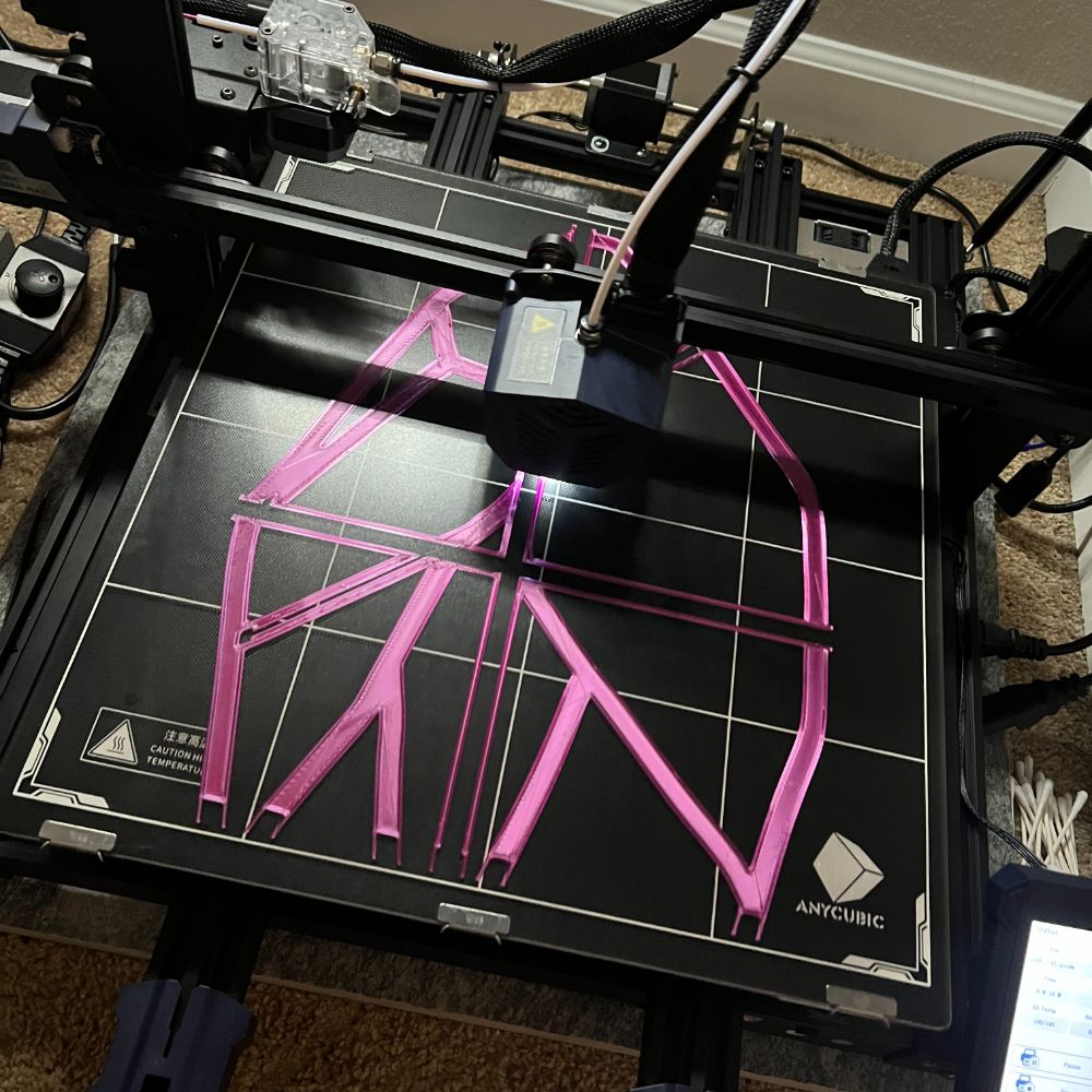
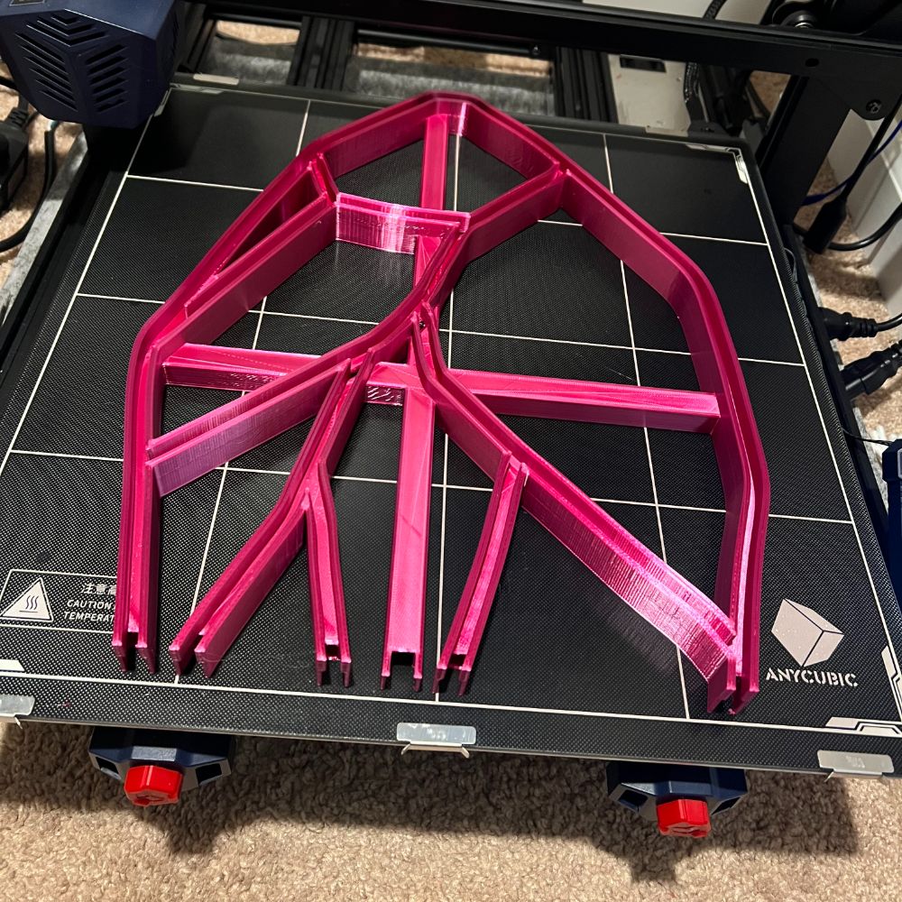
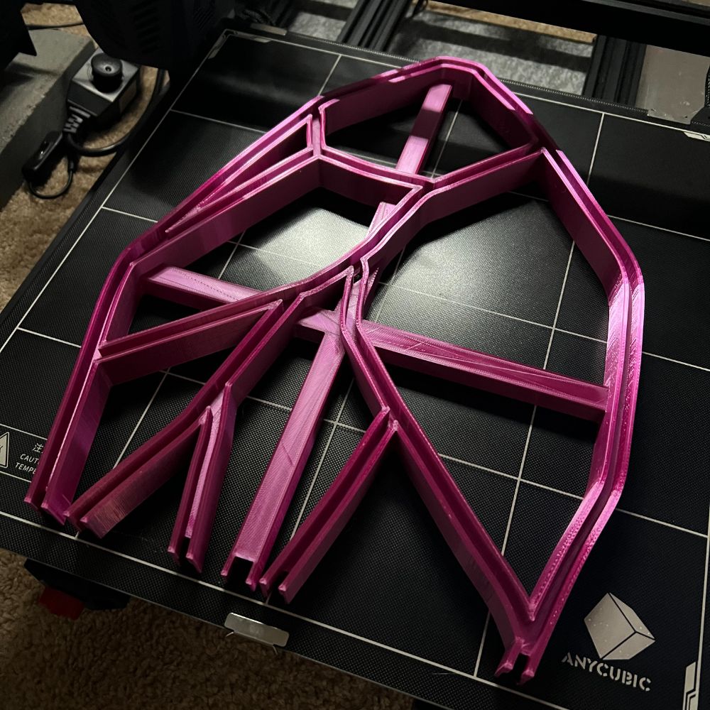
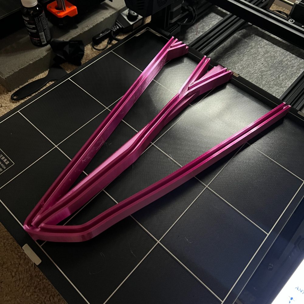
The XBOX360 and GBA designs came out great. The GBA one experienced some extreme edge curling/warping and I figured out why pretty quickly. The closet I run the print farm in gets pretty warm since there’s no airflow in or out, just a vent fan to mix the air around and filter out the microplastics. I opened the door to the closet about an hour before the GBA one finished so the closet could cool off for once, but that caused the print to cool both rapidly and unevenly. For large prints like that, it’s critical that all the layers cool slowly and uniformly so they contract the same amount at the same time. Since I cooled off the closet right as it finished, it was basically the worst thing I could have possibly done. Lesson learned.
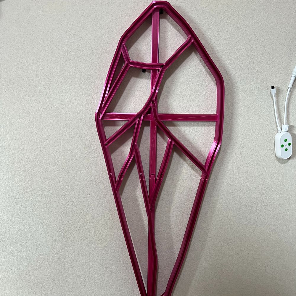
The Dark Crystal design and assembly both came out awesome. It’s one of the most photogenic signs I’ve made so far. Also included in the gallery are some of the portfolio pics I’ll be using.
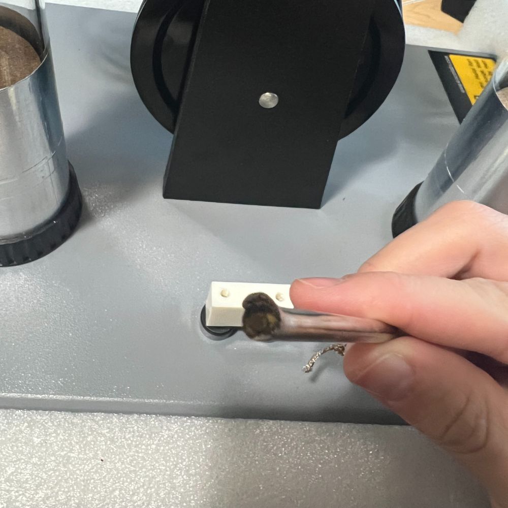
Angel also got me a Wimhurst Generator for Christmas, but it showed up broken. So we ordered a replacement, and the replacement showed up broken in the exact same spot… So maybe sometime soon I’ll have one. During B, I have a basic blacksmithing course that Angel signed me up for which I’m really looking forward to. Hands on metalworking stuff.
Other stuff, I’ve been putting way more time into BJJ as well as studying the Genki books so Angel and I aren’t completely lost in Japan during our trip. My days are mostly working out, studying, or doing mundane repetitive things for money, but I’m pretty happy with it right now.


Aggron
A
For Lab B
Design little housing for FLC
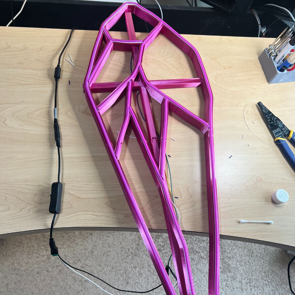
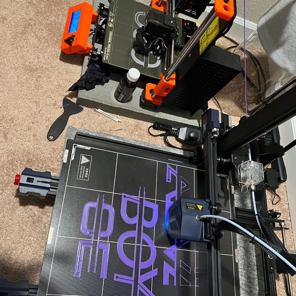
Neon Signs
GORP
GORP
Ramona Repairs
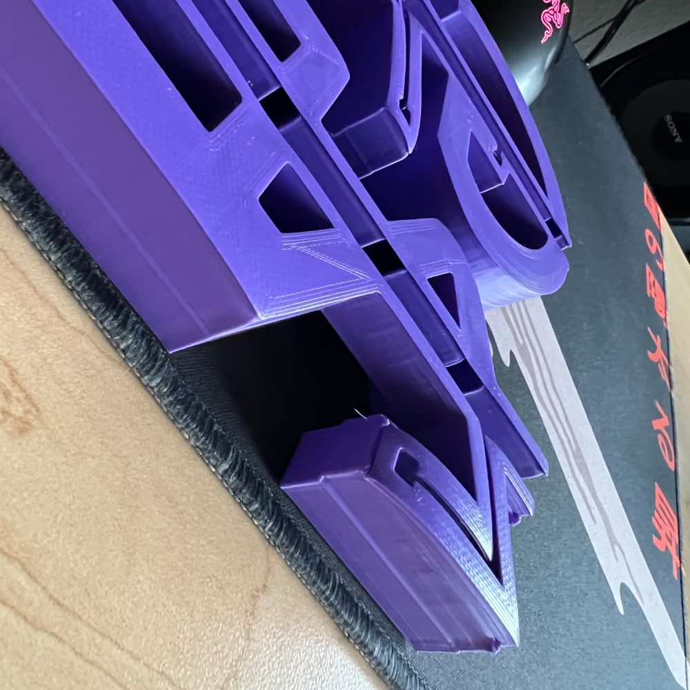
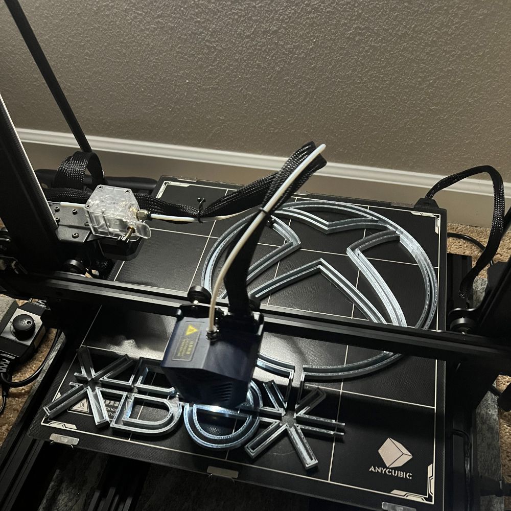
Gameboy Advance
XBOX 360
Dark Crystal
Blacksmithing Course
Jan 21
Breadnet
Fixed breadnet, just added a line to local.rc to launch mosquitto on startup so I can easily fix the mqtt server, which crashes after some time for some reason. Before I had to switch peripherals and monitors and then enter a line into terminal, now i can just toggle the power on the pi and it fixes itself
AOE
Chapter 2
2.1 – Introduction
Notes
A transistor is an active component
Active components amplify
Defined as: the output signal has more power than the input signal
The transistor is the single most powerful resource for interfacing everything in electronics – ICs, circuits, subcircuit modules, etc.
BJTs came first, before FETs in 1947
Simple comparison:
BJTs
Low noise, accuracy
FETs
Low power, high impedance, high-current switching
Transistors have 3 terminals, EBC
Emitter, Base, Collector
Vc – Voltage from collector to ground
Vce – Voltage from collector to emitter
Vcc – refers to positive power supply voltage, usually on collector side
Vee – negative power supply voltage, usually on emitter side
Vcc and Vee probably won’t change polarities if you start working with PNPs though
Transistors are 3 terminal devices, which means there are two voltages and two currents to juggle
Not 3 currents and voltages, because only 2 are independent. the third one is dependent on the other two
2.1.1 – First transistor model: current amplifier
BJTs have three terminals
a small current into the base controls a large current through the collector-emitter
comes in npn and pnp variants
NPN Rules (reverse for PNP)
1 – Polarity
Vc must be greater than Ve
2 – Junctions
Base->Emitter and Base->Collector act like diodes
Base->Emitter diode is usually conducting
meaning base is higher than emitter by at least one diode drop
Base->Collector diode is usually reverse biased
current can’t flow into the base from either E or C
Control current flows into B and out through E
3 – Maximum Ratings
All transistors have max values for
Ic – current flowing through collector-emitter
Ib – current flowing into base
Vce – voltage across collector-emitter
exceed them and it breaks
Other limits worth noting
Max power – Ic * Vce
Max Vbe
4 – Current Amplifier
If 1-3 are followed
Ic is proportional to Ib
Ic = B*Ib
B is Beta which is h_fe
“h parameter transistor model” is no longer popular
PNP Rules
1 – Polarity
Ve must be greater than Vc
2 – Junctions
Emitter->Base is diode
Collector-> Base is diode
Control current flows into E and out through B
3 – Maximum Ratings
4 – Current Amplifier
Beta is a shitty parameter that should not be relied on
Beta varies with
collector current
collector-emitter voltage
temperature
the base-emitter voltage Vbe acting like a diode (rule 2) means you can’t put arbitrary voltages across Vbe
if you put more than one diode drop (0.6-0.8V)
immense currents will flow and probably kill your transistor
For an operating transistor (NPN)
Vb = Ve + 0.6V
For an operating transistor (PNP)
Vb = Ve – 0.6V
Don’t think of collector current in terms of the base-collector diode
the voltages are usually applied in the wrong direction
collector higher than base, diode is Base->Collector
Collector current varies little with Collector voltage
in diode conduction, current rises quickly with increasing voltage – this is not the case with the base-collector junction
to summarize these two diodes
the base->collector one is just there to let you know that collector current can’t go into the base
the base->emitter one is there to restrict Vbe to one diode drop
2.2 – Some basic transistor circuits
2.2.1 – Transistor Switch
If you give the base say 10mA and the beta is 100, then you would expect 1000mA to go through the collector
but that doesn’t always happen
since the emitter is usually connected to ground, Vce is just Vc,
and since the load the transistor (NPN) is powering is usually placed between the collector and the Vcc positive power supply,
the voltage across the load determines how much current will flow through the load and the transistor (collector current)
In order to increase the collector current, Vc decreases
So for LARGE Ic, there’s usually a SMALL Vce
and similarly, for a SMALL Ic, there’s usually a LARGE Vce
Meaning there wouldn’t be a large voltage drop across the load, so the transistor eats up the rest of the voltage to ground by holding it up at the collector
If a transistor needs to provide it’s maximum amount of current, it’s said to enter a state of “SATURATION” and Vc goes as close to ground as it can
This is usually about 0.05 – 0.2V
when you send wayyy too much current into the base, that’s called overdriving
when you overdrive the transistor, it doesn’t blow itself out trying to keep up
the transistor would’ve saturated at 1mA (Beta of 100, Ic = 100mA)
Everything more than 1mA going into the base is superfluous
Note – beta goes down when Vcb is low
Note – add pullup or pulldown resistors
pulldown resistors for NPN – to connect the base with a path to ground when unpowered. this keeps Vbe at zero and prevents conduction
pullup resistors for PNP – to connect the base with a path to Vcc when unpowered. this keeps Vbe at zero and prevents conduction (in this case E is connected to the power supply rails as well)
NPN Base gets switched to positive supply, and some of the current into the base gets routed through the pulldown resistor,
PNP Base gets switched to ground, and some of the current coming out of the base
3 Design tips for Transistor Switches (BJT)
1. Choose the base resistor conservatively to get plenty of excess base current, especially when driving lamps
lamps draw more current when they’re cold
2. If the load is AC or inductive and liable to swing below ground, place a diode Load->Collector in series with the load to prevent the Base->Collector diode from conducting
3. If the load is inductive, protect the transistor with a diode in parallel to the load pointing to Vcc (Parallel Collector->Vcc)
this is called inductive kickback (flyback?)
5 Reasons why transistor switching is superior to mechanical switching
1. transistor switches can be driven electrically from another circuit (interfacing), like from a computer bit
2. transistor switches can enable extremely fast switching speeds (microseconds)
3. you can switch many circuits with a single signal
4. mechanical switches have wear and tear, and they bounce
contactor bouncing
5. remote, cold switching means cables don’t have signals, just DC running through them. this means less signal travel, crosstalk, signal degradation, etc.
Transistor Man
Transistor man’s perpetual task in life is to try and keep Ic = B*Ib by turning a little knob
The knob controls a resistor and he can slide it from
zero ohms, short circuit, saturation, zero Vce
infinite ohms, open circuit, cutoff, max Vce
Transistor three states
Cutoff – High voltage on Vce, No Collector current
Active Region – Some voltage on Vce, Some Collector Current
Saturation – a few tenths of a volt Vce, Max Collector Current
2.2.2 – Switching circuit examples
Notes
A transistor switch is a Nonlinear circuit: the output is not proportional to the input.
After a certain threshold is reached, it abruptly switches from one state to another
The output is not continuous, proportional to the input
In transistor switches, the transistor does not use the active region, it is either in saturation or cutoff
linear circuits contain amplifiers, current sources, integrators, etc and offer more interesting challenges and room for creativity
note, for this section, switch ON means Saturation mode
Switch OFF means cutoff mode
A – LED Driver
Most LEDs are just diodes that start conducting around 1.5-3.5V
A 10-20mA LED will burn your eyes
Because of the Steep IV curve, 5V across an LED will blow it out.
In the basic LED Driver circuit, we use the base resistor conservatively to make sure there’s more than enough base current to ensure the transistor is in saturation
When selecting the collector resistor, we pick a value to set the operating current
Since the LED’s voltage drop is known, and the power supply voltage is known, and we know that the transistor only has a few tenths of a volt across it in saturation (which we can round to zero), it’s easy to pick a resistance for the remaining voltage to set an operating current for the LED
There are ways to devise circuits that provide an accurate output current, independent of what the load is doing (current source configuration)
B – Variations on a theme
Notice the NPN BJT switch circuit connects the load to the positive rail, and the transistor’s switching action makes and breaks a connection to ground.
What if you wanted to connect the load to ground, and use the transistor to make or break a connection to the positive rail?
You would use a PNP switch instead
Why can’t you just put the load on the emitter of the NPN?
Remember that when the switch is ON and the transistor is in saturation, there’s a 1Diode drop between the base and the emitter, and the drop between collector and emitter is nearly zero.
the range of voltage drop across the load is then reduced by 1Diode drop, rather than being capable of full swing (Vcc to Zero)
there are subtler effects concerning the resistance between the emitter and ground not discussed yet, as well an effect where the base and collector current add at the emitter
So the circuit would work, but it’s much better practice to keep the load strapped to positive rails for NPN, and strapped to ground for PNP
PNP switch circuit
the emitter has an arrow pointing INTO the transistor, it’s on the upper part of the symbol, and the emitter is connected directly to positive rail
the collector is on bottom and connects to the load and then to ground
some things that are different
the combined emitter current enters the transistor from the positive supply and forks
the base current LEAVES through the base and then the remainder goes out through the collector. This is what powers the load.
This also means that current won’t be able to flow out through the base until the input signal to the base goes LOW.
That means the PNP switch is an ACTIVE LOW circuit.
When the voltage applied to the base is high (VCC) there’s no voltage difference between Base and Emitter
When it goes low (ground on the resistor), the base will drop 1Diode from the emitter/Vcc, and the rest of the voltage will drop to ground through the resistor.
barebones PNP switch circuits like this can be awkward to work with because the OFF state requires the base be held all the way up at Vcc, which could be 10, 12, 15, 20 Volts. Most control voltages in computers and microcontrollers are either 3V or 5V (called logic level) and so they wouldn’t be able to control a PNP switch as easily as an equivalent NPN switch
In order to get a PNP switch to work with a 3V control voltage, just attach to the base of the PNP switch, another NPN switch.
The NPN switch will receive the 3V, turn on, and when it turns on, it’ll create the high voltage at the base of the PNP switch that’s required to turn the PNP off
Figure 2.10B
R3, 1k, connects Vcc to the Base of the PNP
When the PNP is on, that 1D drop from E to B means that the B node will be at a voltage of 14.4V
Since that is true, the resistor connecting Vcc to B will have to drop 1D as well, meaning it’s current will be low
The resistor below that can be expected to drop the rest of the voltage before the near zero Vce of the NPN
so the remaining 14.4V’s pass through current can be set by the selection of R2
note that this 14.4V current through R2 is a combination of the current through R1, and the base current of the PNP. Most of it will be coming from the base current of the PNP
When the NPN is cut off, and there’s no path to ground through R2, no current will flow through R2 or R3, and the base of the PNP will be held up at 15V.
Once a 3V control signal is applied to the NPN, the NPN will go into saturation, create the path to ground, and allow the base of the PNP to go low enough to allow itself to also enter saturation.
Note that the switch example circuit had the PNP base switching from 15V to 0V. Realistically, one diode drop away from Vcc is all that’s necessary. So it’s just fine that instead it’s going from 15V to 14.4V.
Once the 1D drop on the PNP’s Vbe is established, it goes into saturation and pushes current through the load by creating a connection to the positive rail.
In this case, there are two determinants for the current through the load
1. the Ic=B*Ib, where the base current of the PNP is set by R2
2. the resistance of the load on Q2
C – Pulse Generator – I
for this circuit, before the input signal goes high, the passive, ambient state of the circuit
the initial condition
check the transistors and figure out what state they’re in during initial conditions
Q1 is OFF, obviously, because the input signal has yet to come
Q2 is ON, because R3 creates a direct path to Vcc for Q2’s base
we also know that because Q2 is in saturation, there is a 1D drop for Q2’s Vbe
since the emitter is grounded, that means that Q2’s base is at 0.6V
with this information, it’s easy to calculate the current going through R3, since we have both the resistance and the voltage across the resistance
what’s more interesting is on the other side of the capacitor. since Q1 is OFF, there’s no path to ground there, meaning the Q1 collector node is at Vcc.
There’s no path for current to flow and so there’s no voltage drop across the resistor.
This means that the capacitor has 5V on the left, and is at 0.6V on the right. The Capacitor has 4.4V across it.
Something is going to change once Q1 receives the input signal and opens a path to ground
Since Q2 is ON, in saturation, and a large current flows through it, R4 is there to limit the current passing through so the transistor doesn’t cook
it’s also there to create an output terminal. without the resistor, Vcc would be directly connected to the collector of Q2. What do you measure then if you want an output voltage? It’s just going to be Vcc
This is why resistors can be interpreted as devices that convert currents into voltages. There was no voltage or voltage drop to measure before the resistor was added, just a current.
what happens when the input goes high?
First, the path to ground opens up, dropping the Q1 collector from Vcc to Ground
This voltage drop means there’s now current flowing through R2
two things are true at this point:
the left side of the capacitor is at 0V
the left side of the capacitor is 4.4V higher than the right
because the voltage across a capacitor cannot change instantaneously, the right side’s voltage moves from 0.6V down to -4.4V.
Now, the base of Q2 is at -4.4V and does not meet the 1D criteria and switches off, from saturation to cutoff
because R3 is still connected to Vcc, and its other terminal is now at 4.4V, there’s a 9.4V drop across it, meaning a lot of current is flowing through R3. It doesn’t have a path to ground through Q2, so it has to go through the capacitor
because a current is flowing into the capacitor, the voltage of the capacitor must change. this is the fundamental law of a capacitor.
In this case, a positive current is flowing into the negative terminal, which nullifies the stored charge in the capacitor, lowering it’s stored voltage, rather than increasing it
since one side is fixed at ground, the discharge effect doesn’t change the voltage of the left side, only the right. As the current from R3 flows in, the voltage at Q2’s base slowly increases from -4.4V up past zero (at which point the capacitor begins storing charge again, but with opposite polarity), until it reaches 0.6V again and turns on Q2.
note that during this time, as the voltage on the right side increases, this charging action will decrease the voltage drop across R3, and so the current will taper off too.
It’s important to note that this charging, if uninterrupted by Q2’s reactivation, would continue charging all the way to 5V. At that point, the left terminal would still be at 0, and the capacitor would have a full 5V across it. The current through R3 would slowly reduce to zero, as R3 would have 5V on both sides.
once Q2 turns on, both transistors are on at this point, and both provide paths to ground on either side of the capacitor.
Also, both terminals of the capacitor are locked in place by the two transistors, meaning no current flows through it any more. It still has a 0.6V charge, but that voltage is not changing
If the voltage isn’t changing, there’s no current. this is the rule of the capacitor.
as for the output behavior of the circuit, it’s either 5V or 0V depending on whether Q2 is on or off. If it’s on, then current flows through Q2 and R4 drops 5V, and the output voltage is zero. If it’s off, then no path to ground is available and there’s no voltage drop across R4, so the output voltage is 5
Q2 ON
Vo = 0V
Q2 OFF
Vo = 5V
So the general characteristic is that it creates a pulse of fixed length after receiving one high input swing. in this most basic case, the output is a switch that gets turned up high and remains high indefinitely.
how is pulse length determined?
right away, we already know that the pulse gets cut off by Q2 re-entering saturation once the right side of the capacitor moves reaches 0.6V.
We already established earlier that the left side gets held at ground, so the charging action is taking place on the right side, where current moved through R3 into the capacitor.
This means the time constant for this charging action it t=R3*C
Recall that the charging action starts at -4.4V and would continue charging all the way to 5V if uninterrupted by Q2’s resaturation
So, the duration of the pulse is just the time constant times the time travel factor 5/9.4V (0.53) -> [-ln(1-0.53)]
D – Pulse Generator – II
first, a major draw back of this circuit is that the output pulse has a predetermined length, but it can get cut short if the input goes low again before it’s finished.
the output pulse should be the same regardless of how long the input is high
once we fix this, this means that this pulse generator only triggers on the RISING EDGE
so first, in the cut-short scenario, we send a brief input signal, and q1 momentarily activates, shorting the left node to ground, swinging the right side into the negative voltages, and the capacitor starts charging up towards +5V
before it can charge all the way up to activate Q2 again, the input signal turns off and the capacitor charging curve is reset. no dice
What we need is to keep the left node grounded until the capacitor finishes it’s work
1. what circuit structure can we use to create a conditional path to ground?
an NPN transistor switch
2. what signal in this circuit corresponds to the capacitor indicating it’s done charging?
the output signal of the circuit
it goes high when Q2 is off (while the capacitor is charging)
it goes low as soon as the capacitor is done charging
so what we can do here is take the output signal and plug it into the base of an additional transistor.
Now, when Q2 is Off, the output is HIGH, and so Q3 will be ON
we want the path to ground to be valid while the capacitor is charging (output is high) and so NPN is the right choice here
So we just connect the Q1 collector node to the collector of this new Q3, and now whenever the output voltage is HIGH, this node will be held to ground, regardless of whatever dancing is happening at the input
it needs a little elaboration though. we want to add a resistor between the output node and the base of q3 so there can be a voltage drop. we want the output voltage to stay at 0 and 5 volts, while the base stays at 0 and 0.6V.
without a resistor, they’ll be the same, we want them different, so we split them up
next, we need to look at the currents flowing through these resistors so we can pick the right resistance value to keep everything in line.
we need to consider what states these two transistors might be in to understand what currents are going to flow where and when and how much etc etc.
first, note that we put q3 here to provide a path to ground while the capacitor charges
if the capacitor is charging, that means q2 is OFF and the output is HIGH
if q2 is ON, the output is LOW and will essentially be grounded
This means the base voltage going into Q3 will not be above 1D and q3 remains off
all this means Q2 and Q3 are mutually exclusive
if the output is LOW, we don’t need to consider the currents through the q3 B resistor, because there is none
if the output is high, there will be some current flow through R4 and then through R5 (it will never split and go through Q2 (mutually exclusive)) and then into Q3’s base and out through it’s emitter to ground
so essentially, we have a voltage divider placed between 0.6V and 5V (4.4V to divide).
Some current is going to drain through the q3 base resistor and out through its base when q3 is on. this is unavoidable and will reduce the output’s voltage from 5 (no current flowing) to just under 5 (some current
We want the voltage at the output as high as possible, so we want the second resistor to have a much higher value.
in this case, 20k vs the 1k should be fine
now we can calculate that 4.4V divided into 21k makes about 200uA, and the voltage at the output on HIGH will be around 4.8V vs the original 5V. good enough for us
We could increase this 20k resistance, but then the total current would go down, and that would require a higher Beta value on Q3 for the same performance.
We don’t want to design circuits that are dependent on a specific value of beta, and the lower the minimum necessary the better, since most are around 100.
to check the beta, let’s see how much current needs to flow through the Q3 collector, and how much current is available going into the base
collector sees 5V across 1k, so 5mA or 5000uA
base sees 200uA,
Since Ic = B*Ib, we can calculate that Beta needs to be at least 25 for this circuit
so as long as we can find a transistor with at least 25 Beta and our 5V output is acceptable to 4.8V this is a fine addition to the original design
With the addition of this extra transistor switch creating a new conditional path to ground, the output pulse length is now completely independent of the input pulse length, such that this is now a RISING EDGE TRIGGERED PULSE GENERATOR
E – Pulse Generator – III
There’s still one more deficiency to this circuit to fix
As the capacitor charges up until 0.6V is reached and Q2 turns on the 100us time constant means it will leisurely cross that threshold and slowly activate Q2. meaning the output voltage will not abruptly drop from 5V to 0V, but will decay gradually to the new voltage level
One way of fixing this is to add a schmitt trigger to the output
a schmitt trigger is a circuit that uses hysteresis or regenerative action to turn a slow moving waveform into an abrupt transition
a schmitt trigger consists of two transistors whose emitters are connected to ground through a shared small resistor
then, the secondary transistor’s base is connected to the first transistor’s collector, making it so when q1 turns off and breaks the path to ground, q2 turns on.
both transistors have resistors between collector and Vcc to limit current, obviously.
first, the fact that the shared emitter resistance is small means that both q1 and q2’s base will still be around 0.6V above ground (slightly more, but still not more than say, 1V)
circuit passive state, before input goes high
Q1 is off, Q2 is on, Output is 0V
Q1 is on, Q2 is off, Output is 5V
q1 OFF, q2 ON – mutually exclusive
because q2 is ON, we know that current is flowing through the collector and through the base, combining inside the transistor, and leaving through the emitter.
in this case though, there is a tremendous excess of base current passing through, and a fully saturated collector current.
We know that the voltage at the collector in saturation is near zero, so we can assume a full 5V across the 1k resistor (ignoring the negligible voltage drop on the small shared emitter resistor)
meaning 5mA through the collector
But similarly, we also have 5V dropping to 0.6V on its way to the base. So 4.4V/1k means 4.4mA going through the base and combining to make 9.4mA total going through the small resistor
Note the logic behind the circuit math here is rough and excludes the small emitter resistor until the end
the proper way to do the math here is to use a system of two equations for two unknown variables
Variables
Formulas
Ie
Ie = Ib + Ic
Ve
Ve = 20*Ie
from there, it can be found that Ie = 9.4mA and Ve = 180mV
now because Ve = 180mV, the required base voltage to turn on Q1 is going to be 1D above that, meaning the ON threshold is at 780mV rather than 600mV.
Once that 780mV threshold is reached, the next state of the circuit precipitates quickly.
First, Q1 begins conducting, grounding the collector of q1. This also grounds the base of Q2. So they switch states at the exact same time.
Then, because Q2 is no longer conducting, both the emitter and base currents disappear and are replaced by the singular collector current of Q1 (5mA)
because the current going through the shared emitter resistor suddenly dropped from 9.4mA to 5mA, Ve also drops from 180mV to 100mV
Finally, because the Ve has dropped, the new threshold value moves from 780mV to 700mV.
Because this all happens at the same time, the input voltage is still at 780mV but because the threshold has suddenly decreased to 700mV, the Q1 suddenly becomes fully ON and nearly instantly switches from cutoff to saturation.
The useful property of this circuit is that the moment the ON threshold is reached, the ON threshold suddenly drops such that the transistor has no choice but to instantly saturate. Even the longest of time constants and most leisurely of waveforms will be converted into an abrupt transition
Q1 is on, Q2 is off. The threshold to drop Q1 into the off state is for the input voltage to drop below 700mV.
Similarly, the whole process repeats in reverse for the input FALLING EDGE
The moment the input drops below 700mV:
Q1 stops conducting
the q1e current stops
the q1c/q2b node rises in voltage
the q2b+q2c current emerges
the voltage at Ve goes up
And so the moment the input falls enough to cross the threshold, the threshold is instantly moved back up to 780mV, placing the Q1 base voltage well below the minimum conduction point, and instantly cutting it off, rather than slowly moving out of saturation.
By moving the thresholds in this way, the circuit becomes “sticky” and has “memory” because it “knows” whether it’s on the way up or on the way down
It behaves differently when it’s up or down. the parameters change
this memory effect or state dependence is called hysteresis
An approximate relationship to determine the distance between the two thresholds is
dV ~~= R_e / R_c * Vcc
where the Rc for both q1 and q2 are the same
The RISING threshold is 780mV
The FALLING threshold is 700mV
So they look like this on a number line
<—| [gap] |—->
If they didn’t have the gap, it wouldn’t work. for example if rising was 700 and falling was 780, you’d cross one threshold and then instantly cross the other, it just doesn’t make sense, move on. accept the gap
2.2.3 – Emitter follower (Started A Here)
Notes
The previous circuits were switches, with very nonlinear behavior
meaning, sudden transitions, abrupt on/off states, etc.
The next few circuits are linear, which means the output will be proportional to the input*
*within the intended circuit operating range
an emitter follower is a bjt circuit that follows the emitter
meaning, the emitter is the output
before the output was the collector
now its the emitter
emitter follower
follow the emitter
anyway
also notice that the emitter follower does not have a collector resistor
but it DOES have an emitter resistor
whole thing is flipped around
this circuit is not a switch anymore
because it doesn’t have the collector resistor and emitter straight to ground
it’s an emitter follower
it has an emitter resistor
the emitter can be the output voltage *because* there’s a resistor between the emitter and ground
There is no collector resistor in an emitter follower.
the output voltage is just the voltage at the emitter
and we know that the base voltage is 1D higher than the emitter when the transistor is on
assuming the transistor is on (otherwise this circuit is unpowered and not doing anything)
then we know that the output voltage will be 1D lower than the input voltage or -0.6
Now this seems stupid and this circuit is a waste of space
except remember that we are now dealing with a linear circuit
not a digital/switchy/nonlinear circuit
analog, continuous fluctuations in the waveform of the input are to be expected
we’re now dealing with signals because we’re in linear territory
and so we might have a 2V sinewave that is fluctuating all around
but when we pass that 2V sinewave through an emitter follower, it becomes a 1.4V sinewave
impressive
What happens if the input of the sinewave drops below 1D and the transistor turns off?
Well, the transistor just turns off and nothing passes through
which means that not all of the wave gets passed through
in fact, more than half of the wave doesn’t get passed through.
because a 2V sinewave goes from +2 to -2 and if it stops conducting at +0.6 then everything from -2 to +0.6 (2.6V/4V total) will just be a flatline on the output
this circuit appears more useless by the minute
INPUT AND OUTPUT IMPEDANCE – SOURCES AND LOADS
to understand the value of the emitter follower you need to understand input and output impedance
in electronic circuits, you’re always plugging something in to something else
that is, there are circuit MODULES that are known to have INPUTS and OUTPUTS
MODULES have INPUT and OUTPUT TERMINALS – 2 SETS – BOTH SETS
SOURCES have OUTPUT TERMINALS
LOADS have INPUT TERMINALS
when you have some source, like a power supply, and you connect a motor to it, the power supply becomes LOADED
That is, there is some internal circuitry in the power supply that produces some output voltage, and then there are two TERMINALS for something to connect to that power supply and become part of the circuit
we earlier considered a 10V, 0.1A lamp. Meaning for the lamp to operate properly, it needs 10V dropped across it and 0.1A going through it
We can multiply these numbers together and see that the lamp demands 1W of power
power seems like the right way to analyze how much energy a source is sending out to it’s loads and devices but that’s not how we do it and it’s not as useful
Instead we divide the 10V/0.1A as in R=V/I and turn the lamp into a resistor of 100R.
Now we know that the circuit will behave more or less identically if we replace the lamp with a 100R resistor.
thus, the lamp is considered to be a 100R LOAD onto the circuit
Now, we can estimate what Loads are appropriate for what sources through the analysis of input and output impedance
First, if you’re looking IN to a module, then you are working with its INPUT TERMINALS which means we treat it as a LOAD.
Loads don’t output, they input. They don’t give, they take. Inputs take things. Outputs give things
If you’re looking OUT of a module, then you are working with its OUTPUT TERMINALS, which means we treat it as a source.
INPUT IMPEDANCE = LOAD IMPEDANCE = INPUT TERMINALS
OUTPUT IMPEDANCE = SOURCE IMPEDANCE = OUTPUT TERMINALS
Now in the absolute most abstract sense, when we plug the most abstract source into the most abstract load, we always get a voltage divider.
That is, there’s a voltage source, then the internal source resistance, then the load resistance.
If you want your signal to actually show up across the input terminals of whatever device you’re feeding it to, you need most of the voltage drop to occur on the second resistor, the load resistor.
Another way of saying that is, you want the internal source resistance to be much much lower than the load resistance
Ideally, several orders of magnitude, 2 or 3 is fine
Example, if you have a 10V sinewave source, but the internal resistance and load impedance are both 100R, then only 5V are going to show up in the 100R load.
If you’re expecting 10V and need 10V, you will be sorely disappointed and you will have only yourself to blame for using a source with such high output impedance.
We like small output impedance. We like big input impedance
If you need to remember this, just draw the electronics triangle |>
If you want to go through it, you pass a big wall on the way in, and pass a tiny tiny dot on the way out
BIG input impedance (when acting as a load)
small output impedance (when acting as a source)
Better example, you have a 10V sinewave with a 5R output impedance and you connect a load with 500R input impedance
now, you get 500/505= 99% of your original signal voltage across the load. much better. raise. promotion. brilliant work.
A – Impedance of sources and loads
The Emitter follower’s utility comes from the fact that its input impedance is much higher than its output impedance
It’s a good triangle |>
when used as a load, it has a high input impedance and eats up most of the signal, irrespective of most source impedances
when used as a source, it has a low output impedance, and gives most of the signal it’s sending to the load.
This means a very weak signal that’s not pushing a lot of current or power can pass through an emitter follower, trade off 0.6V from its signal, and receive a tremendous current/power gain.
what was once a weak whisper is now a firm voice. Because the signal going into the base is controlling the flow of a larger output current coming from the 10V source.
Maybe it can power a speaker or something now
Voltage gain isn’t everything
Most of the time we want the source to be “stiff” compared to the load
Meaning, regardless of what load we connect, the source remains the same, or about the same
this can only happen if the source impedance is low enough that any load you might connect is still >90% of the combined resistance and thus received most of the voltage signal
It is always nicer if signal levels don’t change when a new load is connected
Also, in cases where the input impedance of the load can vary with it’s received signal level, then the stiff source always providing the same signal strength regardless of input impedance fluctuations will ensure the circuit can “maintain linearity”
output proportional to input – not freak out and start going all over the place
There are two cases where we don’t want Zin >> Zout
1. Current sources
the whole thing flips
a current source is a source in parallel with its source resistor
the load resistor acts as a parallel resistance and the net resistance between the two has to be calculated in parallel instead of in series.
if you’re using a current source then you obviously want to deliver current to something and so if you have two resistors that need to share one current source, you’d want the load to receive as much as possible and the internal source resistor to receive as little as possible
thus you want the internal source resistance as high as possible, near infinity if you can, and then the load resistance as low as you can, so it takes most of the current from the source
that is, in current sources you want HIGH OUTPUT IMPEDANCE and LOW INPUT IMPEDANCE
2. RF Circuits/Antennas/Transmission
In these cases you want to match impedance and make Zin=Zout
Not the topic right now
B – Input and output impedances of emitter followers
The entire point of the emitter follower is to change the impedance of signals or loads. it doesn’t really do anything else
first, for input impedance, we look at the emitter follower as though it were a load
we consider it’s input terminals and assume it’s connected to some load on the other side already
in order to calculate the input impedance, we want to use V=IR and get R=V/I
So Input Voltage, divided by Input Current
for this circuit, “input” and “base” mean the same thing, because the base is the input
similarly, “output” and “emitter” mean the same thing, because the output terminal is the emitter
but in this case, we’re going to use a small signal variation
to begin with, a voltage change at the base will match a voltage change at the emitter 1:1, so ve = vb
we also know the current formula with ib = B*ic and ie=ib+ic means that
ib*(B+1) = ie
we can now use the relationship
ie = ve/R
and substitute ie with another expression in terms of ib
and substitute ve with another expression in terms of vb
ib*(B+1) = vb/R
vb/ib = R*(B+1)
thus Zin = R(B+1)
where R is the parallel resistance of the native emitter resistor and the attached load
similarly, for the output resistance, look at the outputs of the emitter follower, and assume it is attached to a source
the best way to analyze this is to force a change in the output voltage, and analyze how that changes the output current, input voltage, and input current.
note that there are two parallel paths to ground from the output node: one through the emitter resistor, and one through the transistor. the transistor usually has much lower resistance, and so the net resistance is determined by the lower and we can ignore the emitter resistor
in this case, we assume the voltage source is fixed, and the input voltage is still vb. the input current is vs-vb/rs, but since we’re only considering changes in current, we can say
ib = -vb/rs
similarly, ve/r=ie, ie=(b+1)ib
putting these together and getting ve/ie (output voltage/output current)
ve/rs = ie/(B+1)
ve/ie = rs/(B+1)
Zout = rs/(B+1)
where rs is the source resistance into the base
Exercise 2.5
5V source from a 15V supply that varies no more than 5% under a full load of 25mA
Use a voltage divider to set the voltage, and then an emitter follower to increase the output impedance
use 5V and 25mA to determine a min load of 200R
note that 5V drops <5% during full load conditions
select an emitter resistor, and determine total emitter current during NL and FL conditions
once NL and FL ie are set, assume a low beta and determine the necessary base current under both conditions
next, find Vb by adding 1D to the output voltage of 5V
now, design a voltage divider taking into account the slight current draw into the base
make sure to change the voltage at Vb for the 5% drop during FL conditions
calculate R2 first, and then combine the currents to find R1
R1 has a drop of 9.4V from 15->5.6
C – Follower drives switch
this has utility in circuits like the LED driver in Fig 2.16
a normal transistor switch requires the signal can push at least the LED current divided by the Beta of the transistor to drive it
by taking that same transistor switch circuit and strapping an emitter follower to the input, the emitter follower can now amplify that signal’s current and now a current in the microamps can drive the LED.
This is a good example of how we push control signals down to extremely minimal power levels by using transistors to amplify appropriate to the context.
D – Important points about followers
In this situation, there’s a negative power supply instead of ground connected to the emitter through a resistor.
Since the load resistor is connected to ground, this effectively forms a negative voltage divider.
Assuming the two resistances are equal, that means that, when the transistor is OFF (Vbe < 1D) the voltage divider sets the output voltage to -5V.
Since the NPN Emitter Follower can only SOURCE current, there is no way for the transistor to SINK any of the current flowing from ground through the resistors and down to the -V.
If it could sink the current, then the current sinked would go through the transistor, stealing it from the emitter resistor. If the emitter resistor’s current went down, then so would it’s voltage drop and the voltage at the output node would necessarily decrease to voltages lower than -5V.
In this case, the lowest possible voltage for the output signal is -5V, when the transistor is simply OFF and not doing anything.
When the transistor is ON, the output voltage is obviously and necessarily 1D lower than the input voltage.
The input and output V/t curves show the output being a waveform of slightly less amplitude owing to the 1D drop, and then for the -5V limit, the input can go down to -10V, but when it does, the output will simply flatline at -5V until the input rises above -4.4V again (1D above)
this is called Clipping
so the limitations of an npn emitter follower are
asymmetrical current drive capability aka clipping
DONT UNDERSTAND
The emitter follower has a low value of small-signal output impedance
The emitter follower has a much larger large-signal output impedance (up to Re)
The output impedance switches from small signal to large signal at the point where the transistor goes out of the active region.
A low small-signal output impedance doesn’t imply a large output current capabilty
A Push-Pull configuration using both npn and pnp can be used.
This issue also comes up when the emitter follower is driving a load that has it’s own sources, which can then force a current in the wrong direction
This happens often in power supplies, where the output of one power supply is an emitter follower, and then it goes and drives, of course, another power supply
Base-Emitter Breakdown
reverse breakdown for the base-emitter junction is usually small, around 6V
so if Vbe swings to -6V or deeper, the transistor is likely to get damaged or destroyed
This also can result in permanent B reduction
A diode pointing to B between E and B [E >| B] can allow current to flow from the higher E to the lower B, and lock the reverse bias to 0.6V, which is a safe level
Gain is slightly less than unity
Gain is not quite 1.0, because Vbe is not constant and depends on Collector Current
This will be addressed in the Eber Molls Section
2.2.4 – Emitter followers as voltage regulators
The simplest regulated supply of voltage is a zener diode, powered through a resistor from the source
Zener diodes eat all unloaded current and have a minimum demand for their services
Design for worst case scenarios
If Vin fluctuates, use the lowest value. Does the output, regulated voltage supply still meet spec?
What if Iin also fluctuates? If it goes up, the voltage drop across the resistor leading up to the zener also goes up. Does the voltage supply still meet spec?
Ex 2.6
zener set to 10V, from a 20-25V supply. load current 0-100mA. zener demands 10mA
what R
what power rating on zener
zener is a shunt regulator
limitations
vout not precise
moderate ripple rejection and regulation against load changes
iwde varying currents require zeners to handle dissipation at low load current levels
Figure 2.21
by strapping an emitter follower to the zener, performance is improved
first, the emitter follower ensures the output voltage is 0.6V lower than the zener setpoint
second, the load the zener sees is now reduced by a factor of B
Just connect the npn to the same power supply as the zener, and now there’s a much better, more regulated circuit, with lower and more consistent power dissipation.
to limit the amount of current going through the transistor, add Rc
make sure the voltage drop across Rc is less than the voltage drop across Rz
That is, make sure the collector doesn’t fall below the base
if the ripple in the zener circuit is still too much you can always just add a lowpass filter to the zener’s bias circuit (R)
2.2.5 – Emitter follower biasing
Notes
If the emitter follower is being driven by an earlier stage in the circuit, they’re probably sharing a power supply.
If they’re sharing a power supply, it’s usually okay to simply connect the output of the prior stage directly to the base of the emitter follower.
One issue where this doesn’t work is if the signal coming into the base is capactively coupled.
Signals that are capacitively coupled have an average value of 0V (no DC Offset) and so swing negative. For the typical emitter follower stuck between Ground and +VCC, this means that the entire negative half of the swing is going to get clipped
The first and fastest way around this is to simply set up a voltage divider at the base, and then connect both the base and the capacitvely coupled signal together in the middle of the voltage divider. This will set the new zero-point of the signal to the midpoint between Ground and VCC.
This process of selecting the characteristics of the circuit when there is no signal being applied (Zero-Point of the signal) is called Quiescent Point
In most cases, the Quiescent Point is chosen to allow maximum symmetrical signal swing of the output waveform without clipping
However, because we’ve effectively added another module to our emitter follower, we now need to consider terminal impedances
The output impedance of the voltage divider should be small, compared to the input impedance of the emitter follower
The essence of selecting these impedances can be boiled down to:
The current flowing in module A should be much higher than whatever is drawn by module B
And the main advantage of the emitter follower is that it can pass a signal while drawing very little current for itself. It’s input impedance is extremely high (B*Re)
R1//R2 << B*Re
A – Emitter follower design example
Now to put this all together
We want to design an NPN emitter follower.
We want it to receive an AC coupled signal.
We want it to pass out an AC coupled signal
The signal will be an audio signal with frequencies [20Hz-20kHz]
VCC is +15V
Quiescent Current is 1mA
The structure is an input signal capacitor joined with a biasing voltage divider, feeding the NPN emitter follower, whose output is then also capacitively coupled to the next stage
The process is as follows
1. Set bias point to 50% of VCC
This part is easy. VCC is 15 so we want the bias at 7.5V.
Note that the bias point refers to the output voltage, not the input voltage
Since the emitter is at 7.5V, the base must be 1D higher at 8.1V.
2. Choose an Re value to create the Quiescent Current called for using that 50%
Since the emitter is at 7.5V, the base must be 1D higher at 8.1V.
To get 1mA from the output voltage at 7.5V, we want 7.5kR
3. Choose Divider Values (note Base current draw makes divider imperfect)
Assuming a Beta of 100, the quiescent current draw into the base should be 10uA.
Recall the loading criteria from earlier. The current drawn by the base should be much lower than the current flowing through these divider resistors
More specifically, the parallel resistance (output impedance) should be at least 10x smaller than the input impedance of the emitter follower.
Since we have selected Re already, and assumed a Beta, it’s easy enough to say that the input impedance into the emitter follower will be 7.5k x 100 = 750k.
The parallel resistance should thus be 1/10 of that, 75k.
At this point, we have that the voltage divider should output 8.1V and that their parallel resistance is 75k. Calculating their values is tedious but trivial.
If they were 50-50 and equal, then their ratio would be 1.
In this case, the first resistor drops (15-8.1)V and the second drops 8.1V
so 6.9 and 8.1
The current flowing through them is usually equal, but not exactly in this case, since some small current is getting pulled into the npn base. this means that the second resistor has less current in it than the first resistor. We have designed this so that that difference in current is trivial though, so we can ignore it and assume they’re still equal.
now, assuming the currents are the same in both resistors, we can safely assume that the ratio of the voltage drops is also the ratio of the resistances.
The ratio is 1.17
Now, we can set up a parallel resistance equation with the upper resistor as X and the lower resistor as 1.17*X, all set to 75k
we get about 130k and 150k
4. Choose C1 to set a high pass filter with its load
An RC high pass filter looks like a capacitor and then a resistor. In this case, we have a capacitor at the input terminal, and then a complicated circuit that can be reduced to a simple resistance. This high pass filter will determine what signals enter the module so it’s highly relevant to make sure we don’t muck up our signal before it goes anywhere
Because the node the capacitor is connected to can flow to both the voltage divider AND the emitter follower at once, we treat their impedances in parallel.
we’ve already determined that the impedance looking both out and into the voltage divider is simply the parallel of the two resistances. that’s 75k.
we’ve also already determined the input impedance into the emitter follower. that’s 750k.
Putting 2 and 2 together, we get a parallel impedance of 75k/750k = 68k
Now we can abstract away this circuit and work on our high pass filter
We know that this RC HPF is an incidental consequence of us capactively coupling the input signal into the circuit, so we don’t want it to attenuate any of our input signal.
Which means we should make sure the entire range of it is after the highpass 3dB point
Our input range is 20Hz to 20kHz, so let’s set the corner frequency to 15Hz to be safe.
From here, we can use the f=1/(2*pi*R*C) formula and solve for C, since we already have f and R.
C = 0.15uF.
5. Choose C2 to set a high pass filter with the output load
Since C2 is forming a second HPF with the output, we consider the load’s value
We’re already assuming that the load will always be bigger than Re
So, for a minimum load value of Re, we can calculate C2 using the same frequency as before, 15Hz
Note that for higher load values, the corner frequency will actually go further down below 15Hz
Also Note that for cascaded high pass filters like this, both capacitor values should be increased slightly to compensate for the increased attenuation
6. Output impedance
Finally, with all values set, we can calculate the final output impedance of this entire circuit
From the output node, there are three paths:
1. Unconnected output to load through C2
2. Ground through Re
3. Ground through npn (through R1, R2, and Source)
Putting this together, the output impedance must be the emitter resistance in parallel with the 1/B factored triple parallel resistances of the two voltage divider resistances and the output impedance of the source that drives this circuit, which we can assume a value of 10k for.
Zo = (Re) // (1/B*[R1//R2//Zin])
A few principles from this example:
The Base-Emitter Junction can be treated as a viable path to ground when calculating input and output impedance
However, if you pass through it, a factor of B will be applied.
If you move from emitter -> base, then everything on the base side needs to be factored by 1/B, from the emitter’s perspective
Similarly, if you move from base -> emitter, then everything on the emitter side needs to be factored by B, from the base’s perspective
Voltage Dividers can be used to bias emitter followers, but they will become imperfect, since some gate current needs to be drained away from R2 and into the base.
This imperfection can be more or less ignored as long as the current running through the divider is ordered higher than the base current
capacitive coupling on both input and output can result in cascaded/stacked filters, which should be treated with caution. f=1/2piRC is essential.
When biasing an AC coupled signal, bias the base to ensure the emitter is at 50%VCC after the 1D drop
B – Followers with split supplies
Another way to get around having to do all this biasing nonsense and just pass a signal through an emitter follower is to have split supplies. That is, a positive and a negative supply rail.
Since AC signals are usually “near ground” and have no DC offset, connecting the emitter to a negative supply instead of 0 gives the emitter follower some negative range to work with.
Warning: base current path to ground
most circuits will assume that the signal source going into the base of the npn will have its own path to ground.
Either way, best practice is still to provide one. This usually takes the form of a resistor connecting the base to ground.
This discussion is relevant when there are symmetrical supplies, because the emitter doesn’t have a connection to ground. Before the base current could go through the BE junction and find its way to ground, but with symmetrical supplies the base needs it’s own path to ground
Perceptive Moment: now the signal/input current moving into the base has two pathways to divvy up current into. It’s easy enough to see that Rb and B*Re are the two options, and so, set Rb to be 1/10th of B*Re
C – Bad biasing
If resistances get multiplied by B when passing through BE anyway, can’t you just set up a voltage divider by strapping a resistor from VCC to B that is 10x the resistor from E to GND?
eg. 750k -> VCC-Base
7.5k -> Emitter-GND
This assumes a value of 100 for the Beta. This circuit only properly divides the voltage and sets the quiescent point at 50% VCC if beta is 100.
Beta changes from transistor to transistor and on the temperature and on what color socks the president is wearing today. Relying on it and designing your circuit around it is a recipe for disaster. Don’t do it.
Using a stiff voltage divider makes the quiescent point of the circuit independent of fluctuations in Beta.
D – Cancelling the offset – I
a PNP emitter follower is similar, but since the arrow is pointing inwards and the emitter is on top and expected to be more positive,
the collector is on the bottom of the symbol and connects directly to ground. the emitter is on top of the symbol, points in towards the base, and connects to VCC through the emitter resistor.
In this case, the emitter follower is on and active as long as the base is 1D LOWER than the emitter.
Meaning that the output of the PNP emitter follower, at the emitter terminal, is 0.6V higher than the input signal.
So if you just put two of these together, PNP then NPN and match the emitter resistors, no problem. Offset Cancelled (RIP Offset)
Note that if you don’t have symmetrical supplies, you’re still going to experience negative side clipping despite the cancellation
note that Vbe varies with a number of things and this will be slightly imperfect. If you need perfect, use an opamp
2.2.6 – Current source
A – Resistor plus voltage source
You can make a current source by using a voltage source and a resistor in series with the load terminal
The only thing is, the voltage has to be huge and the source resistor has to be huge, so huge that the addition of the load resistance is trivial.
That is Rs+Rl =~ Rs
This source resistor also experiences large power dissipation, which is another issue
Note that when dealing with voltage sources, we talk about loads in terms of the current they’re going to draw
when we are dealing with current sources, we talk about how much load voltage instead
Since after all, for a constant current, the bigger the load resistor, the higher % of the total resistance between source and load resistance it’ll occupy, and thus the more voltage drop it’ll take
Ex. 2.9
if you wanted a current source to remain constant within 1% over a load range of 0-10V, that is a different way of saying, how big does a voltage source need to be for a 10V fluctuation to account for less than a 1% change?
1000 Volts, across a 1K source resistor, results in a 1A current
If another resistor is added such that the 1K source resistor now takes 990V and the load 10V, the current will decrease from the added resistance
It’s easy enough to calculate what this new reduced current will be since we already have the voltage drop across a known resistor: 990v/1000r = 0.99A. a 1% reduction in amperage for a 10V load
B – Transistor current source
Due to a supply shortage of 1000V power supplies and 1kW resistors, we have had to come up with alternative methods for sourcing stable currents (this is a joke)
It’s much easier to make a current source out of a transistor.
take an npn, give its base a voltage, calculate the 1D drop to the emitter, run a resistor from the emitter to ground
Picking the input voltage and the emitter resistor sets the current flowing out of the emitter
Technically, Ie=Ib+Ic, but in this case we can say Ie=Ic as long as the beta is high enough. a 100 Beta means the difference between Ie and Ic is only 1%
From there, we can just attach our load between the VCC and the collector. The current flows through the load as determined by our transistor/emitter resistor and voila.
C – Current-source biasing
So now we just have the problem of how to set that voltage.
Can we use a voltage divider again? yea sure
Remember to keep it STIFF. that is, the output impedance of the voltage divider needs to be small compared to the input impedance of the current sourcing transistor circuit.
Remember the triangle |>: small output impedance, large input impedance
for a voltage divider, the output impedance is always just the two resistors in parallel.
For the npn, the input impedance is B*Re. (remember there is no meaningful path through base-collector, so our load does not factor in here!)
There are other fun ways to set the voltage too, like using a zener, or even just stacking Diodes until the N*1D is where you want it
D – Compliance
Current sources can only provide constant current for some range of load voltages.
An earlier example could range between 0V and 10V for the load voltage and keep the current accurate to within 1%.
For these simple transistor current sources, the main criteriea is that the transistor remain in the active region.
This is qualified by the Collector being at least 0.1V above the emitter.
in 2.32A, the emitter is at 1.0V, so the collector has to be 0.1V above that. the lowest voltage the collector can go to is them 1.1V.
VCC in this case is 10V
If there were no load and the collector could connect directly to VCC and the VCE would be 10->1 = 9V
As the load varies, the voltage drop across the load can increase or decrease, but that voltage drop can’t expand so much that the collector drops below 1.1V.
This means that the maximum load voltage is 10-1.1=8.9V.
So this current source is COMPLIANT for [0-8.9V] and will provide approximately constant current for all loads in that voltage range
In the event that the load has its own supplies or batteries or sources or what have you, it can actually act as a voltage source that INCREASES the voltage at the collector. This is fine for the most part, but every transistor will have a maximum Collector-Emitter breakdown voltage.
E – Cancelling the offset – II
you can use the same PNP-NPN emitter follower offset cancellation structure here in the current source as well.
After all, the only difference between an emitter follower and a current source is
a load connected between VCC and the Collector
The emitter takes in and passes an input signal, the source doesn’t
one is POWER, the other is CONTROL oriented
This makes it simple and clean
Vin is approximately equal to emitter voltage on Q2. So you just set the second emitter resistor and input voltage and the load will see that current. It’s as easy as I=V/R now
F – Deficiencies of current sources
It’s not perfect, but it’s better than looking for the fabled 1kW resistor
2.2.7 – Common-emitter amplifier
Notes
As mentioned previously, the Emitter follower is a CONTROL type circuit, which takes in and passes out a signal
The current source is a POWER type circuit, which supplies energy, but doesn’t deal with signals or information really
We are now going to combine them
This combination of both power and control characteristics is called the Common-Emitter Amplifier
to begin with, take the classic transistor current source, and give it a load resistor.
Next, we are going to capacitively couple a signal into this current source at the base.
But in order to do this, we’ll also need to add a voltage divider for biasing.
At this point, we have the transistor with its emitter resistor, a collector resistor acting as a load, two resistors forming a voltage divider on the base, and then a capacitor for coupling the input signal.
Since this is intended to act as a current source, we don’t actually want to bias it to 50%VCC. The output isn’t the emitter terminal anyway, it’s actually the collector. More on this in a moment
The collector’s voltage isn’t related to the base or emitter voltages so directly as a 1D drop.
We can see that the voltage at the collector terminal is just VCC subtracted by whatever voltage gets dropped through the collector resistor
That is
Vc = VCC – Ic*Rc
VCC is known, and so is Rc, since we picked it already
Only thing left is Ic
We can assume a high Beta and that Ie=Ic.
Thus, since Ie = Ve/Re = Ic,
We can bias the base, set Ve, and then pick Re to set the emitter current, which is also the collector current
Now to actually Bias it.
Use this ability to set the Ic and Rc to put the collector at 50%VCC
Now the stage is set.
We inject a wibbling signal in via the input capacitor, causing the base voltage to wibble.
The rule is that Ve is always 1D lower than Vb while active, and this wibble is small and doesn’t deactivate the transistor.
This means that Ve also matches the wibbling of Vb
And if Ve is changing, that means that the current going through Re is also changing.
And since the emitter current is equal to the collector current in this case, that means the voltage drop across the collector resistor is wibbling too.
Finally, the Collector voltage is wibbling.
It’s worth noting though, that since for Vc to go UP, the collector current has to go DOWN (reducing the voltage drop in the collector resistor and bring the collector terminal closer to VCC),
The relationship is negative. That is, the signal comes out flipped upside down
Derivation of the same
vb=ve
ie = ve/Re
ie = vb/Re
ie = ic
ic = vb/Re
Vc = VCC – Ic/Rc
vc = -ic/Rc
ic = vb/Re
vc = -(vb/Re)*Rc = -vb*(Rc/Re)
vc = output
vb = input
vc/vb = Gain
vc/vb = -Rc/Re
Gain = -Rc/Re
This is called a
Common-Emitter Amplifier with Emitter Degeneration
A – Input and output impedances of the common-emitter amplifier
The most important concept here is remembering that there is no meaningful path from collector to base. the resistance is measured in the megaohms
To summarize
Base -> Emitter: multiply by B
Emitter -> Base: divide by B
Base -> Collector / Collector -> Base: A brick wall
Collector -> Emitter: this path routes through the Base ergo, Brick Wall
Input Impedance
Signal comes in, sees three paths to ground
1 through R1
1 through R2
1 through the BE junction and down through Re
Thus, Zin is R1//R2//B*Re
Output Impedance
From the output, two paths to ground
1 through Rc
1 through the brick wall (Megaohms)
Since they’re in parallel, we ignore the brick wall and say it’s just about Rc.
Note that the output impedance for the common emitter amplifier is determined by the collector load resistor
The emitter follower from earlier’s output impedance was determined by the parallel paths of Re and (1/B)*[everything on the input side].
Since the 1/B side is almost always much lower then Re, the output impedance of the emitter follower is independent of the emitter resistor (load resistor for the ef)
Output Impedance
Common Emitter Amplifier
Dependent on Load Resistor (Rc)
Emitter Follower
Independent of Load Resistor (Re)
2.2.8 – Unity-gain phase splitter
Notes
A phase splitter generates a signal and its inverse, the upside down one.
The common emitter amplifier by default only puts out the inverse, but it’s possible get the upright one out of it
First, set the gain to unity by making the collector and emitter resistors exactly equal.
Now, the voltage drop across both of Rc and Re will be equal
Meaning the signal measured at the collector will be the upside down one, but the signal measured at the emitter terminal will be the right side up once, since it’s being measured from ground
also note that if you were to measure VCC with the collector output as the REFERENCE (GND) you’d see the upright signal. but this isn’t meant to inform design decisions. Just reminding you that everything is relative to a reference point
Now that the phase splitter is active, we want to bias it carefully so that both signals have enough room to swing without clipping or slipping the transistor into saturation.
If you have a signal that goes up and down, then you want the quiescent point collector voltage at 0.75VCC, so that it can stretch 0.25VCC in either direction, to 1.0VCC or 0.5VCC
Since the voltage drops will be the same, this also means that the emitter terminal will rest around 0.25VCC and then fluctuate up to 0.5VCC or down to 0
A – Phase shifter
This part is black magic
Since we have two signals, and they’re the inverse of eachother, if you were to measure the difference between them, you’d just get a double amplitude version of the signal
but if instead, we bridge the two signals with an RC, and measure the middle voltage, we’ll find that the new output is the same signal, with the same amplitude, but phase shifted by
theta = 2*atan(w*R*C)
And so we replace R with a potentiometer so we can change the angle of the phase shift
R=0 -> theta=0
cue phasor diagram
V+ and V- form unit vectors that point in opposite directions, forming a line of length 2.
Vc and Vr are vectors that travel from the tip of V+ to V-, and are required to be at right angles.
Note that Vc is flexible as well as Vr, since it’s not Xc, but Vc. R can dominate the voltage drop and leave little left for C. Vc can shorten.
Finally, this technique is useful but a little crude due to loading effects. the resistor can’t get too big. Later on, there will be improved phase splitter effects using Opamps
2.2.9 – Transconductance
Notes
There were a few steps to the common emitter amplifier
a
applied base voltage wibble results in an emitter voltage wibble
b
calculating emitter current, ignore base, determining collector current
c
calculating the collector voltage swing
The amplifier can be broken into two sections
First Section: everything but the collector resistor
the INPUT is the base voltage
the OUTPUT is the emitter current
Thus, the GAIN = OUTPUT/INPUT
GAIN has units of Current/Voltage
I/V = 1/R, thus the units are CONDUCTANCE
therefore, the first section is a TRANSCONDUCTANCE Amplifier
In this case, the gain is just -1/Re
If Re is 1k: you can input 1V and you’ll get 1mA
That is, I(V) = (1/Re)*V
I(1.0V) = (1/1000[A/V])*(1.0V) = .001A
transconductance gain is “gm”
Second Section: the collector resistor
the INPUT is the collector current (equal to emitter current)
the OUTPUT is the collector voltage
Thus, the GAIN has units of Voltage/Current, which is Resistance
V/I=R, Thus the units are RESISTANCE
therefore the second section is a TRANSRESISTANCE Amplifier
In this case, the gain is Rc
V(I) = Rc*Ic
V(1mA) = (10,000)*(1mA)
V(1mA) = 10V
transresistance gain is “rm”
And so the transconductance section converts a voltage to a current
and then the transresistance section converts a current back to a voltage
overall gain is the product of the two gains
Gv = gm*rm
Gv = -1/Re * Rc = -Rc/Re
You can analyze them separately as well, replacing transconductance circuitry with a different circuit topology with a similar value of gm
You can also change the load part and check gain versus voltage swing, there are tradeoffs there as well.
An active load/current source can have a transresistance of 10,000V/A or more
A – Turning up the gain: limitations of the simple model
If you reduced Re, the -Rc/Re would imply that gain would rise without limit at Re -> 0 but that doesn’t happen. Cue Eber Molls
B – Recap: the “four topologies”
So far, we’ve seen 4 circuits
Transistor Switch
Switch: no emitter resistor, load on collector
Emitter Follower
Control: no collector resistor, emitter resistor to set current, output on emitter
Current Source
Power: emitter resistor to set current, collector on load
Common Emitter Amplifier
Power+Control: emitter and collector resistors, output on collector
2.3 – Eber-Moll model applied to basic transistor circuits
2.3.1 – Improved transistor model: transconductance amplifier
Notes
For many applications, there is no need for an advanced model of the BJT
Switch, Current Source, Follower, Amplifier
Now it is time to dive deeper
The previous model of the BJT was as a current controlled current source
That is, current in, current out
Ic = B*Ib, to be specific
Input, Ib, Output, Ic
Now we’re looking at it as a transconductance device:
Voltage in, current out
Ic as a function of Vbe
The applications for this more specific modeling include
differential amplifiers
logarithmic converters
temperature compensation
etc
all fancy higher precision analog stuff
NEW RULE #4
When rules 1-3 are obeyed, the following relationships are true:
Vt = kT/q
Ic = Is(T) * [e^(Vbe/Vt) – 1]
Vbe = Vt * ln[ (Ic/Is(T)) + 1]
notes
The current passing through the collector
Is a scaled version of Is(T)
Is(T) is the saturation current, which varies from transistor to transistor, and also varies by temperature
the scale factor is e raised to the power of the ratio of the base emitter voltage to the ambient thermal voltage
Thermal voltage is the ambient voltage present in the transistor at a given temperature, and Vbe gets ratio’d by that in order to determine how much current passes through
Vt – Thermal Voltage
q – electron charge constant
1.60×10^-19 C
k – Boltzmann’s constant
1.38×10^-23 J/K
T – absolute temperature
K
Old Rule #4 (pre-Ebermolls)
If 1-3 are followed
Ic is proportional to Ib
Ic = B*Ib
B is Beta which is h_fe
“h parameter transistor model” is no longer popular
New Rules
NPN Rules (reverse for PNP)
1 – Polarity
Vc must be greater than Ve
2 – Junctions
Base->Emitter and Base->Collector act like diodes
Base->Emitter diode is usually conducting
meaning base is higher than emitter by at least one diode drop
Base->Collector diode is usually reverse biased
current can’t flow into the base from either E or C
Control current flows into B and out through E
3 – Maximum Ratings
All transistors have max values for
Ic – current flowing through collector-emitter
Ib – current flowing into base
Vce – voltage across collector-emitter
exceed them and it breaks
Other limits worth noting
Max power – Ic * Vce
Max Vbe
NEW RULE #4
When rules 1-3 are obeyed, the following relationships are true:
Vt = kT/q
Ic = Is(T) * [e^(Vbe/Vt) – 1]
Vbe = Vt * ln[ (Ic/Is(T)) + 1]
notes
The current passing through the collector
Is a scaled version of Is(T)
Is(T) is the saturation current, which varies from transistor to transistor, and also varies by temperature
the scale factor is e raised to the power of the ratio of the base emitter voltage to the ambient thermal voltage
Thermal voltage is the ambient voltage present in the transistor at a given temperature, and Vbe gets ratio’d by that in order to determine how much current passes through
Vt – Thermal Voltage
q – electron charge constant
1.60×10^-19 C
k – Boltzmann’s constant
1.38×10^-23 J/K
T – absolute temperature
K
Old Rule #4 (pre-Ebermolls)
If 1-3 are followed
Ic is proportional to Ib
Ic = B*Ib
B is Beta which is h_fe
“h parameter transistor model” is no longer popular
Vt = kT/q
Ic = Is(T) * [e^(Vbe/Vt) – 1]
Vbe = Vt * ln[ (Ic/Is(T)) + 1]
Note that in the transistor’s active region, Vbe >> Vt, and so the result of the exponential becomes high enough that the -1 can be ignored in the formula for Ic
Ic = Is(T) * e^(Vbe/Vt)
The value that determines the collector current is actually base-emitter voltage
Beta was just a rough approximation
this new formula is also accurate over a wide range of currents, nA to mA.
If you map the actual Ic vs Beta, that’s called a Gummel Plot
Typical Gummel plots look like a wide flattish hill, meaning Beta decreases at extreme ends. It’s most stable from 10^-7 to 10^-2 A
Or, 100nA to 10mA – stable beta range
2.3.2 – Consequences of the Emers-Moll model: rules of thumb for transistor design
Notes
Some simple and handy “Ratio Rules” to help calculate changes in Vbe and Ic
Ratio Rule #1 – Change in Vbe
Ic2/Ic1 = e(dVbe/Vt)
the ratio of the new current over the old current
is equal to the exponential of the change in Vbe divided by Vt
Ratio Rule #2 – Change in Ic
dVbe = Vt*ln[ Ic2/Ic1 ]
the change in base-emitter voltage
is equal to the natural log of the ratio of the new current and the old current, scaled by the thermal voltage
A – The steepness of the diode curve.
using these ratio rules, it’s easy to derive that, to 10x collector current, we only need to increase Vbe by ~60mV.
Four More Shorthands
1
10xIc -> dVbe = +60mV
2
2xIc -> dVbe = +18mV
Ic doubles every 18 mV
3
4%dIc/1mv
every mV increases Ic by 4%
4
Ic = Ic0 * e^(dVbe/.025)
dVbe in Volts
B – The small-signal impedance looking into the emitter, re, for the base held at a fixed voltage.
now to do something awful and take the derivative of one of these formulas
Vbe = Vt * ln[ (Ic/Is(T)) + 1]
we’re going to calculate the derivative of Vbe with respect to Ic
That is, if the base voltage is constant, how do Ic and Vbe influence eachother?
dVbe/dIc = will also be units of incremental Resistance, dR
actual math
by doing a u-substitution and natural log derivative, you’ll get
[Vt + 1/Is] / [(1/Is * Ic) + 1]
We can assume the +1 is irrelevant
and then we can cancel the 1/Is
We’re left with
Intrinsic Emitter Resistance – re
re = Vt/Ic
Where Vt at room temperature is usually 25mV so either
re = 0.025/Ic (Ic in Amps)
or
re = 25/Ic (Ic in mA)
Note that this formula can be inverted and instead of representing resistance it can represent conductance
gm = Ic/Vt
if in mA and mV,
gm = 40*Ic
C – The temperature dependence of Vbe.
Even though the Vbe equation scales directly with temperature,
Is(T) scales with temperature inversely, stronger than that
To the point that Vbe actually decreases with temperature overall
Handy Rules
at constant Ic, Vbe decreases 2.1mV/C
at constant Vbe, Ic increase about 9%/C
D – Early effect.
at constant Ic, Vbe varies slightly with changing Vce
dVbe = -N*dVce
N usually around .0001 to .00001 (10^-4 to 10^-5)
Ic = Ic0 * (1 + Vce/Va)
Another way to express it is in terms of Early Voltage Va
Early voltage comes from this expression
N = Vt/(Va+Vce)
which then simplifies to
N = Vt/Va
2.3.3 – The emitter follower revisited
Notes
To summarize all of the changes and finnicky interdependencies:
Formulas:
Vt = kT/q
Ic = Is(T) * [e^(Vbe/Vt) – 1]
Vbe = Vt * ln[ (Ic/Is(T)) + 1]
Ic = Is(T) * e^(Vbe/Vt)
Four More Shorthands
1
10xIc -> dVbe = +60mV
2
2xIc -> dVbe = +18mV
Ic doubles every 18 mV
3
4%dIc/1mv
every mV increases Ic by 4%
4
Ic = Ic0 * e^(dVbe/.025)
dVbe in Volts
Handy Rules
at constant Ic, Vbe decreases 2.1mV/C
at constant Vbe, Ic increase about 9%/C
Early effect
at constant Ic, Vbe varies slightly with changing Vce
dVbe = -N*dVce
N usually around .0001 to .00001 (10^-4 to 10^-5)
Ic = Ic0 * (1 + Vce/Va)
Another way to express it is in terms of Early Voltage Va
Early voltage comes from this expression
N = Vt/(Va+Vce)
which then simplifies to
N = Vt/Va
Intrinsic Emitter Resistance – re
re = Vt/Ic
Where Vt at room temperature is usually 25mV so either
re = 0.025/Ic (Ic in Amps)
or
re = 25/Ic (Ic in mA)
or
gm = Ic/Vt
if in mA and mV,
gm = 40*Ic
Summary
Vbe now determines Ic
Beta is still in play
increasing Vbe increases Ic
constant T
increasing temperature decreases Vbe
constant Ic
increasing temperature increases Ic
constant Vbe
increasing Vce decreases Vbe
constant Ic
Increasing Vce increases Ic
constant Vbe
add an intrinstic resistor in series at the emitter
re = Vt/Ic
Generally speaking, we just say re = 25 @ 1mA
re = 2.5 @ 10mA
re = 250 @ .1mA
and so on
The source impedance of the emitter node specifically (with fixed base voltage) will just be the change in Vbe wrt to the change in Ie
But since Ie ~ Ic
dVbe/dIc = re = Vt/Ic = 25/Ic
The source impedance of the emitter node specifically is re
The reason the emitter follower has sub-unity gain is because the intrinstic emitter resistance forms a voltage divider with the load, and eats up some of the voltage on the way down
Eber Molls effect on the Input and Output Impedance of the Emitter Follower
Since there is now a tiny resistor attached to the emitter, any load connected to the emitter will be forming a voltage divider between re and RL
Output/Source Impedance
2 parallel Paths to ground from the output node (unloaded)
1
through RE
2
through re, bjt, source resistance, voltage source
Meaning the overall output impedance can be expressed as
Zo = RE // [re + (1/B+1)*Rs]
Input/Load Impedance
From the input node, the signal passes through the BJT
Then through the intrinsic emitter resistance
From there, there are two paths to ground, RE and RL
So, the overall input impedance is
Zi = (B+1)*[re+(RE//RL)]
2.3.4 – The common-emitter amplifier revisited
Notes
If the common emitter amplifier has an emitter resistor
this is called “Emitter Degeneration”
Which is pretty dramatic terminology for something that just reduces the gain a little in exchange for stability
Recall that gain for the common emitter amplifier was
Gv = -Rc/Re
now we know that Re will never be zero, but will at least be re = 25mV/Ic[mA]
this means that the gain will fluctuate like crazy with output current.
If we add a large resistor to drown out the re, like 1k or 10k, the gain will obviously go down, but it will remain stable for a larger range of currents
So as long as there’s the external emitter resistor present, we can usually just ignore re
There is another case though where you parallel the RE with a capacitor
Now, high frequency signals can ignore RE and go straight to ground, which means they’re concerned primarily with re.
That also means that re will form an RC filter with the RE-parallel capacitor
If we have a common emitter amplifier, without an emitter resistor, we will not have infinite gain
Similarly, if we measure the input impedance, we know that it’s not zero now, because that tiny re is there.
Zin is now going to be (B+1)*re
“common emitter” and “grounded emitter” are sometimes used interchangeably, to refer to when there’s no external emitter resistor. RE = 0
the “common” means ground. more specifically. the input and output share the same ground
base and emitter, share the same ground
and they both have a path to ground
the collector, no path to ground
A – Shortcomings of the single-stage grounded emitter amplifier
1. Nonlinearity
Simple 10k Collector resistor, no emitter resistor
Gv = -Rc/Re
Re = re = 25/Ic
Gain varies from -800 down to zero between 2mA and 0mA
Awful performance
Poor linearity, tons of distortion
This thing could be useful with some feedback
Without feedback, it’s only useful for small signal swings around the Q point
ONE MORE TIME
The emitter degenerated common emitter amplifier
Adds Re >> re
Such that the gain becomes effectively independent of Ic
Incremental Gain & Distortion & Nonlinearity
Several new concepts here on the grounded emitter amplifier
First
Incremental Gain
The quiescent gain is
Gv = -Rc/(25/Ic_q)
Where Ic_q is the quiescent current
Flipping this around we get
Gv = -Rc*Ic_q/25
the 25 is Thermal Voltage, Vt
and Rc*Ic is just Vrc – the voltage drop across the collector resistor
In this case, we’re specifically talking about the quiescent voltage drop
Obviously, the voltage drop across the collector resistor will change with collector current, etc.
Gv = -Vrcq/Vt
Now we can say that the gain is equal to the ratio of the voltage drop across the collector resistor, to the thermal voltage
Now, for incremental gain
Since Vrc is variable, we can say this is a function
Gv(Vrc) = -Vrc/Vt
and so the incremental gain dGv is determined per volt of dVrc and the 1/Vt factor
dGv = -dVrc/Vt
Nonlinearity
Nonlinearity can be quantified as the fractional change of gain with swing
fractional change of gain referring to gain increasing by 10% or something proportional like that
These changes in gain are proportional, so they’re referenced back to the quiescent Gain, so
(Ginst – Gq)/Gq
and swing referring to the distance between an instanteous voltage and the quiescent voltage
Since after all, signals push voltages up and down and move it away from the quiescent point. This distance from Vq is referred to as swing.
Specifically, instantaneous swing
But it’s not just the raw voltage difference, it’s also fractional, referred back to the quiescent voltage drop
That is, swing is (Vinst-Vq)/Vq
Also expressed as dVout/Vdrop in the book
Putting this together, we get our expression for nonlinearity:
dG/G = dVout/Vq
Distortion
Finally, distortion
If distortion is present, that means the signal is not perfectly linear
A perfectly linear signal has no distortion
Therefore, the measure of distortion is to take the waveform, subtract the strictly linear part, and whatever is left is the distortion
the amplitude of whatever is left is the quantity of distortion, and we measure that as a fraction of the total amplitude of the waveform.
Meaning we might get numbers like 5% distortion
For some reason I do not understand, we divide the number by 3 and say that’s the distortion
so 1.66% distortion if you calculate 5
It’s important to be clear, nonlinearity and distortion are two different ways of talking about the same thing in this context.
That is, to calculate distortion, just solve the dG/G from earlier
If gain moves from 200 to 204, you can calculate distortion right then and there
(204-200)/200 = 4/200 = 2%
2/3 = 0.7
0.7%
Even adding just a 225R resistor to the emitter will drastically improve linearity.
It comes at the price of reducing quiescent gain by 10x though
Example, given a fluctuating triangle input, you can calculate gain
use the input voltage, and our rule of thumb of +4% IC per 1 mV+
IC Changes, the voltage drop across Rc changes, and from there gain can be calculated
a simple 10V supply, 5V output bias, 5k resistor circuit being fed a 25mV triangle wave is going to have its gain flying all over the place
>20% distortion and such
2. Input Impedance
Because the signal source impedance and the amplifier’s input impedance form a voltage divider, the grounded emitter amplifier will experience further nonlinearity
if the emitter is directly grounded, then
Zin = B*re = B*25/Ic
3. Biasing
You might think you can use the eber molls equation to bias the grounded CE amp (GCEA) to some fine tuned Vbe,
But since Vbe is roughly proportional to 1/T, that means even small changes in temperature will cause the transistor to saturate.
fixed Vbe, Ic rises 10x for a 30C temperature rise
Vbe: 2.1mV/C
Ic: 9%/C
Ic: 10x / 30C
B – Emitter resistor as feedback
The transistor is a TRANSCONDUCTANCE DEVICE
Gain is in terms of A/V
Input is a voltage, output is a current
Input into the amplifier is Vin, measured from Ground
AKA Vb
Output is collector current Ic
We convert this current back into a voltage using a Transresistance device, a resistor
it converts current into voltage, and then we measure the voltage and back-calculate the current using the gain of the transresistance device (resistance of the resistor, measured in Volts/Amp)
Negative Feedback involves taking some portion of the output and feeding it back into the input
It costs some gain to have but improves many characteristics like linearity
adding an emitter resistor is a form of negative feedback
Input is VB, but that’s not what fully determines IC
What fully determined IC is VBE
Which is VB – VE
This means the input is modified, it’s subtracted by some term VE
But VE is not a static value
VE actually changes according to the output, IC – making it a sample of the output
What’s more, the emitter resistor actually serves the same tranresistance conversion role as the collector resistor.
The collector resistor converts the output current into an output voltage that’s easier to measure and pass around
the emitter resistor converts the output current back into a voltage so that that sampled voltage can then be subtracted from the input, VB in the form of negative feedback.
The circuit diagram may not show a complete loop being formed but negative feedback is present in this circuit, since a portion of the output is fed back into the input.
2.3.5 – Biasing the common-emitter amplifier
Notes
If you need high gain and so don’t want to do feedback, there are a few more options
A – Bypassed emitter resistor
Since the amplifier is meant to amplify signals, which are AC and not DC
You can just add a capacitor in parallel to the emitter resistor and then bypass it
the capacitor’s impedance decreases with frequency, so its presence means AC circuits pass through the intrinstic emitter resistance, and then have a free short to ground and can freely ignore the emitter resistor
DC can’t ignore that capacitor and has to go through the emitter resistor
This is useful, because we can have a small emitter resistor providing gain that is high and stable, while still allowing the actual signals to pass through unimpeded. The gain remains high because the voltage at the emitter remains above ground due to the emitter resistor.
You can’t have the emitter voltage too low. Something like 0.2 is too low, because fickle variations in Vbe will cause Ve to fluctuate in dramatic proportion to its total value.
If Vbe climbs from 0.6 to 0.625, Ve will drop 10%, and so will Ie. Not a good situation
Keeping Ve up to around 1V is sufficient for most cases
The whole system is more stable if you use two resistors and add the capacitor bypass for the second one though, forcing the current to pass through the first resistor.
This helps further stabilize Ve, while still retaining the benefits of increased gain at signal frequencies
bypassed emitter resistor means stable biasing without change in gain at signal frequencies!!
1/10th of whatever Vc is a good guideline for Ve
Note that if you’re going to add a bypassed emitter resistor structure like this,
When you go to calculate the input impedance of the amplifier, (for the RC filter formed by the input coupling capacitor and the input impedance of the rest of the amplifier)
you need to do it AT SIGNAL FREQUENCY
Meaning that emitter resistor is getting bypassed and not factored into the signal frequency level input impedance
you can also put 1 R in parallel with an RC series.
The lone R sets the DC bias point
The R in RC lets you set the signal-level gain
B – Matched biasing transistor
Sometimes, you can buy a chip that has two transistors in the same monolithic package
That is, two transistors, one stone.
This means that the transistors will always be the same temperature, and so temperature effects will be negated
I mean, obviously the normal temperature effects are still in play, like overheating it such that saturation occurs. But you don’t have to worry about one transistor getting hotter because it’s moving more power, and then its Vbe and Ic and all that start shifting around, etc.
C – Feedback at dc
You can add a voltage divider at the bases, but instead of connecting it to VCC like a normal person you can be a little freak and connect the top back to the collector
If the emitter is grounded, this means the middle of the voltage divider will for sure be 1D. BUT, if, for example, the divider ratio was 10:1, that means that 1D drops on R2, and then 10x1D drops on R1.
This forces the collector to stay up at ~11x1D with reasonable efficacy
This is cool, but the R1 resistor now serves as a path from the input to the output and so the input impedance is reduced pretty dramatically
D – Comments on biasing and gain
since Gain is
G = -Rc/Re
and the grounded emitter amplifier has just
re = 25/Ic
Why not just increase Ic so the re gets lower, and the gain goes up?
Well, if you want to increase the gain but keep your quiescent voltage
the higher current means you’re going to have to use a smaller resistor for Rc in order to maintain the same voltage drop across Rc
In fact, you can prove that the Gain of a grounded emitter amplifier biased to 0.5Vcc at the collector has a Gain limit of G=20*Vcc independent of quiescent collector current
Exercise 2.16
Design a tuned common emitter amplifier stage to operate at 100kHz. Use a bypassed emitter resistor and set the quiescent current at 1.0mA. Assume Vcc = +15V and L = 1.0mH, and put a 6.2k resistor across the LC to set Q=10 to get a 10% bandpass. Use Capacitive input coupling
First, the layout of the circuit
A Common Emitter amplifier has three zones: the load at the collector, the emitter, and the biasing circuit
the load at the collector is going to consist of an RLC parallel circuit
this RLC will form a bandpass filter
the emitter is going to have a parallel R//RC for the bypassed emitter resistor
one resistor to set the DC bias at the emitter terminal/DC Gain
and an RC to set the gain for signal frequencies
the base is going to have a normal voltage divider for base voltage biasing, and then a standard input capacitor as well
Next, the sequence of approach
There are five areas that need solving
A
Use given R, L, Q, and f to solve for C in the RLC
B
Select a VE, and RE for emitter bias and DC gain
C
Select R, C, and f in the emitter-bypass to pass signal frequencies
D
Bias the base voltage divider and supply ample base current
E
Select Cin by analyzing the overall High Pass Filter formed by Cin and the Input Impedance Zin of the entire circuit
A B and C can all be done first, D has to be done after B, and E has to be done last
If you can do this problem quickly and accurately, you have a good grasp of what’s going on
2.3.6 – An aside: the perfect transistor
2.3.7 – Current mirrors
Notes
A current mirror is easy to make
But you do need a matched transistor
Thankfully, in the world of ICs, matched transistors in single monolithic packages are plentiful
Here’s what you do.
Take a transistor, PNP example
Connect VCC to emitter on top
Connect Resistor through Collector down to ground
Connect Base to Collector
Now base current flows in through E->B, creates voltage drop 1D
Now Base and Collector are both VCC-1D
voltage goes through resistor and makes current IP = VCC-1D/RP
By selecting R we select the current
Now, since we have a matched transistor, and their properties are identical at all times, any Vbe we apply to the second transistor will result in an identical Ic on the other side, Thanks Eber-Molls
So we just connect the Base-Collector node to the base of the other matched transistor
Now all that’s left is to connect a load for the current source to source current through, on the other side.
If we need to change the current, we just change the programming resistor
the second transistor doesn’t get a say in the current, it just samples the Vbe of the leader.
Note, resistor goes on the opposite side of the B-E junction, always on the collector
E straight to supply rail
A – Current-mirror limitations due to the Early effect
Now, we know the VCE for Q1 in the current mirror circuit is just going to be VCC down to 1D.
In this case, 15 -> 0.6V = 14.4V is the VCE for Q1
However, the VCE for Q2 won’t necessarily be the same
Because the current is set, a wide range of load resistances can be selected and the current source will be compliant
But since V = IR, the load resistance and the output current together form the collector voltage, which won’t necessarily be 0.6V.
This means that VCE is liable and almost guaranteed to be different from the VCE in Q1
And we know from the Early Effect that VBE to maintain a fixed current actually changes dependent on VCE
Meaning the currents won’t be exactly equal, but that level of precision is not needed
You can improve the performance of this by adding matching emitter resistors that drop a few 10ths of a Volt or 1V. This negates the effects of small variations of Vbe and Vce on the output current
B – Wilson mirror
If you pay close attention
In NPN BJTs, the base current flows into the base, and combines with the collector and the sum moves out through the emitter
in PNPs, the emitter points inwards, and contains the sum of currents
Once it enters the emitter, the base current forks off and flows OUT through the base terminal
Where does this base current go?
In the current mirror, the two PNP transistors have their bases connected. Obviously these two base currents don’t just combine and cancel out. They would cease to flow and be currents in that event.
The connection that ties the two bases down to the Q1 collector will be where the two base currents flow out through
meaning, the current seen by the Rp programming resistor is actually higher than the collector current
It’s actually Ic + 2xIb
The load resistor is Ic + 0xIb, so the currents are not equal both due to early effect and due to the base current error
The wilson mirror is a clever solve for this
After the two base currents recombine, just add another transistor before the load resistor, a PNP. This PNP will take one of the base currents from the entrance at the emitter and pass it out through it’s base back over to the top of the programming resistor.
Now the programming resistor is seeing Ic + 1xIb
The current leaving this Q3 new transistor will still have one of the two Ib’s with it, so leaving the collector of the Q3 and entering the load resistor is also Ic + 1xIb
Thus, the base current error is exactly cancelled!
Hooray!
LEFT ON PAGE 102
2.3.8 – Differential amplifiers
A – Biasing with a current source
B – Use in single-ended dc amplifiers
C – Current-mirror active load
D – Differential amplifiers as phase splitters
E – Differential amplifiers as comparators
2.4 – Some amplifier building blocks
2.4.1 – Push-pull output stages
A – Crossover distortion in push-pull stages
B – Thermal stability in class-B push-pull amplifiers
C – “Class D” amplifiers
2.4.2 – Darlington connection
A – Sziklai connection
B – Superbeta transistor
2.4.3 – Bootstrapping
2.4.4 – Current sharing in paralleled BJTs
2.4.5 – Capacitance and Miller effect
A – Junction and circuit capacitance
B – Miller effect
2.4.6 – Field-effect transistors
2.5 – Negative feedback
2.5.1 – Introduction to feedback
2.5.2 – Gain equation
2.5.3 – Effects of feedback on amplifier circuits
A – Predictability of gain
B – Input impedance
C – Output impedance
D – Sensing output current
2.5.4 – Two important details
A – Loading by the feedback network
B – Phase shifts, stability, and “compensation”
2.5.5 – Two examples of transistor amplifiers with feedback
A – Circuit description
B – Analysis
C – Series-feedback pair
2.6 – Some typical transistor circuits
2.6.1 – Regulated power supply
2.6.2 – Temperature controller
2.6.3 – Simple logic with transistors and diodes