
1/16/2023 – 1/29/2023
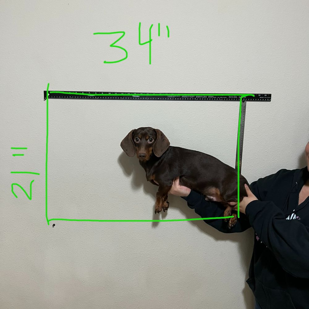
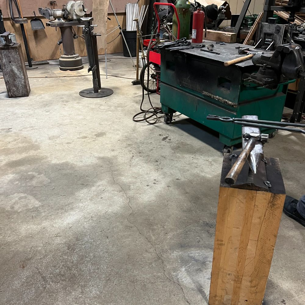
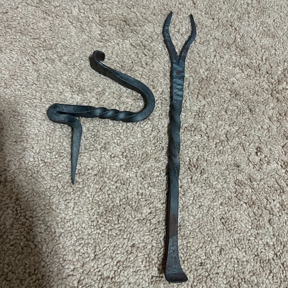
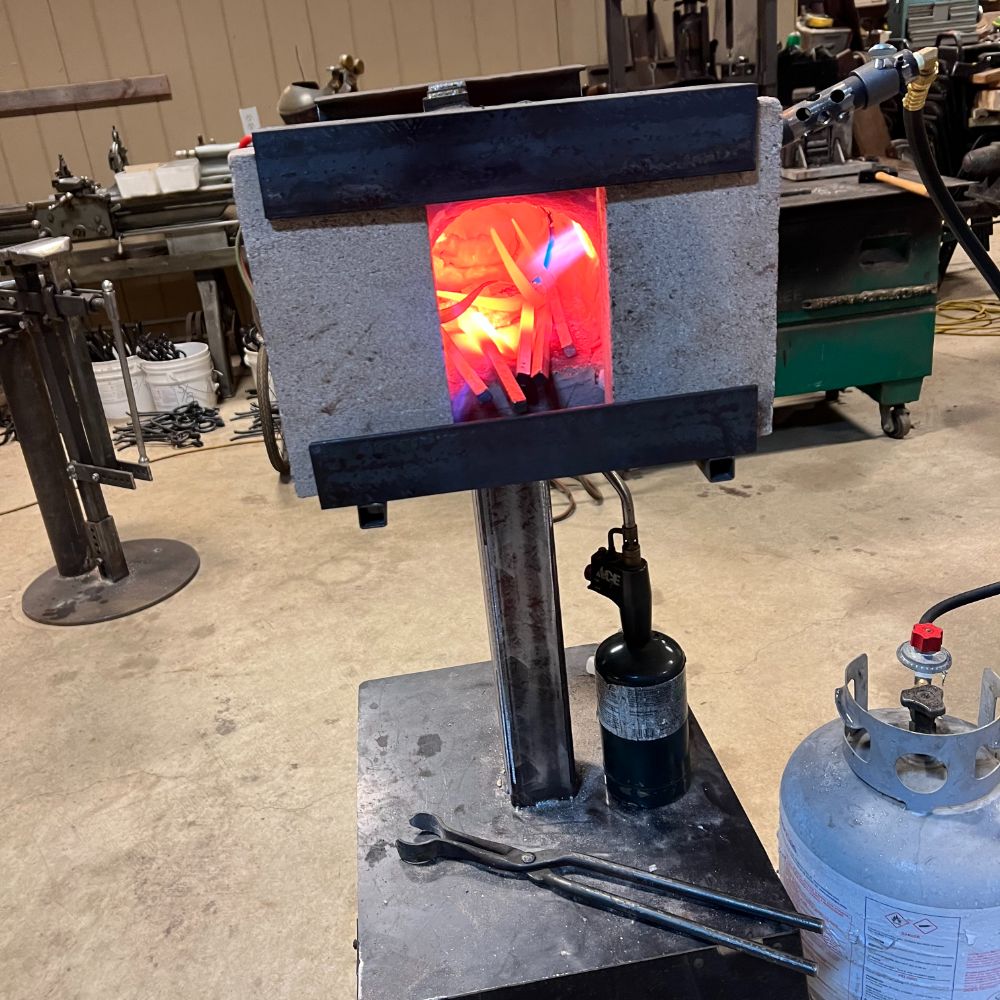
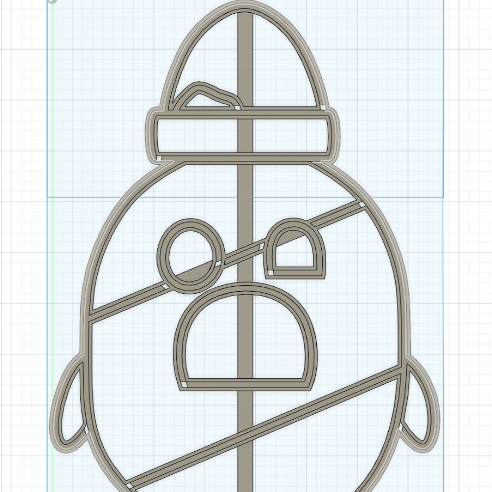
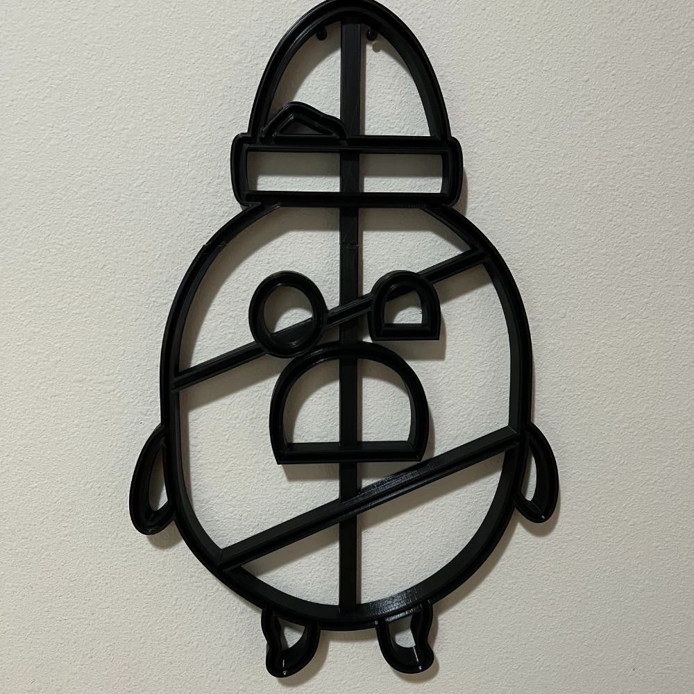
Summary: Still mainly focused on the signs. Didn’t read as much AoE as I was hoping for. Made a portfolio and opened up for new orders, got a few more pretty quickly, then things slowed down a little but I’ve got work to do and am making money again. Angel signed me up for an all day basic blacksmithing course for Christmas, and I went on Saturday. It was fun and I learned a lot but Blacksmithing is definitely not my thing. It is SO MUCH HAMMERING.
I kind of slowed down in week 2 so I’m focusing more on AoE for C.
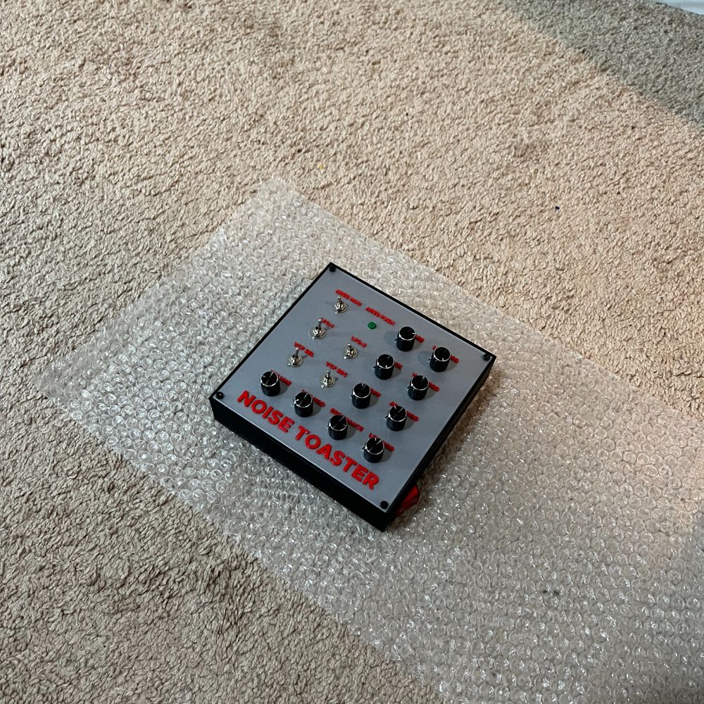
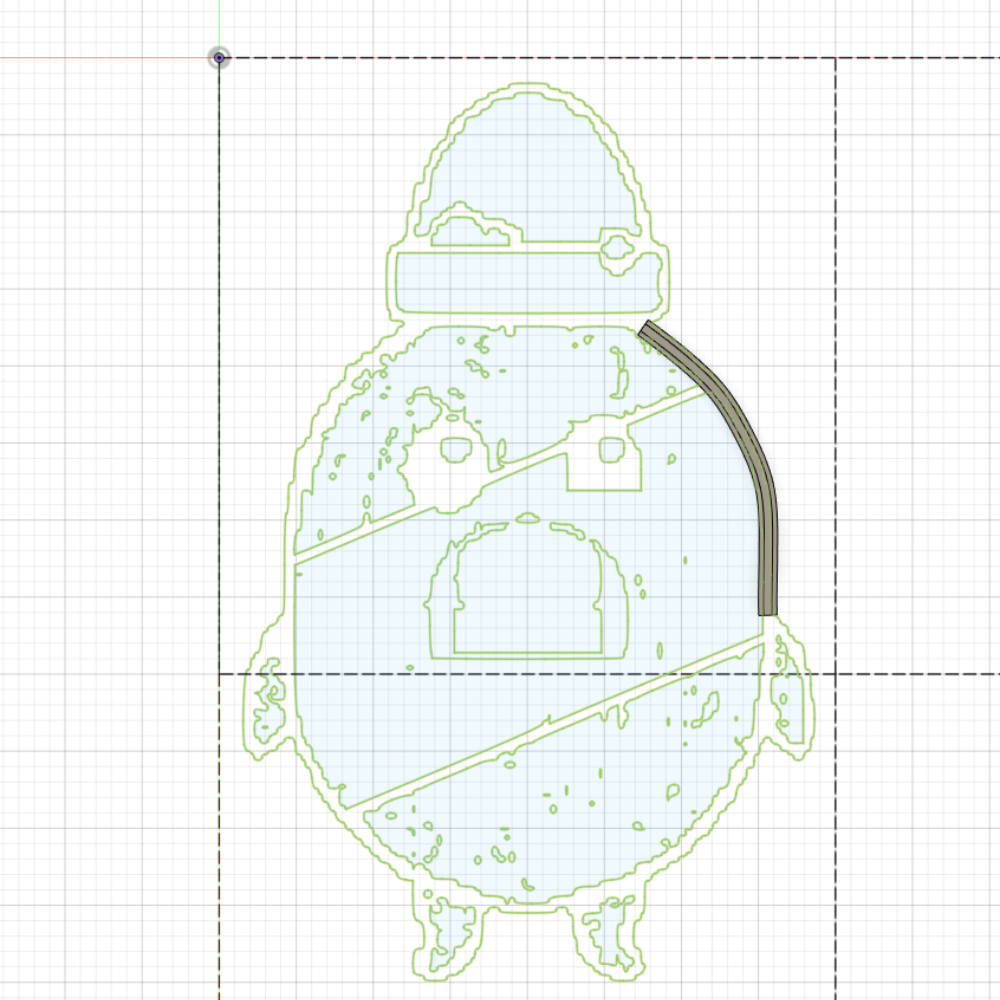
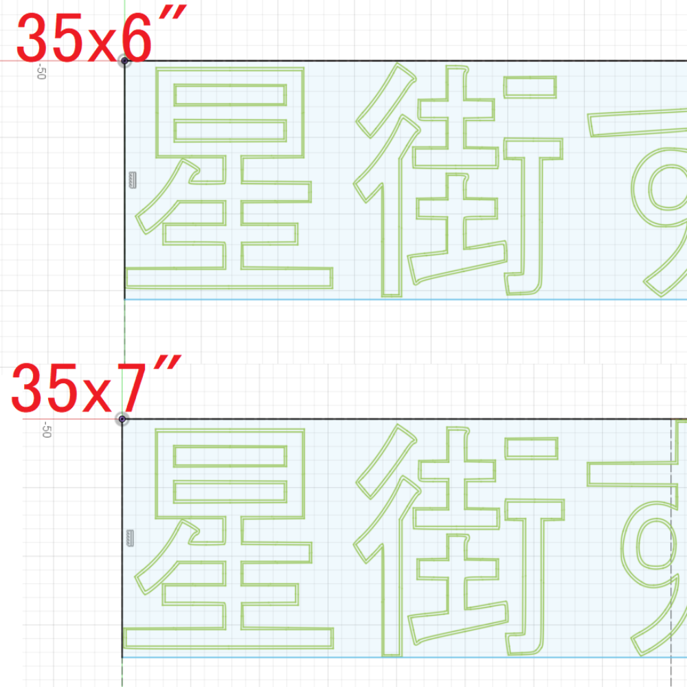
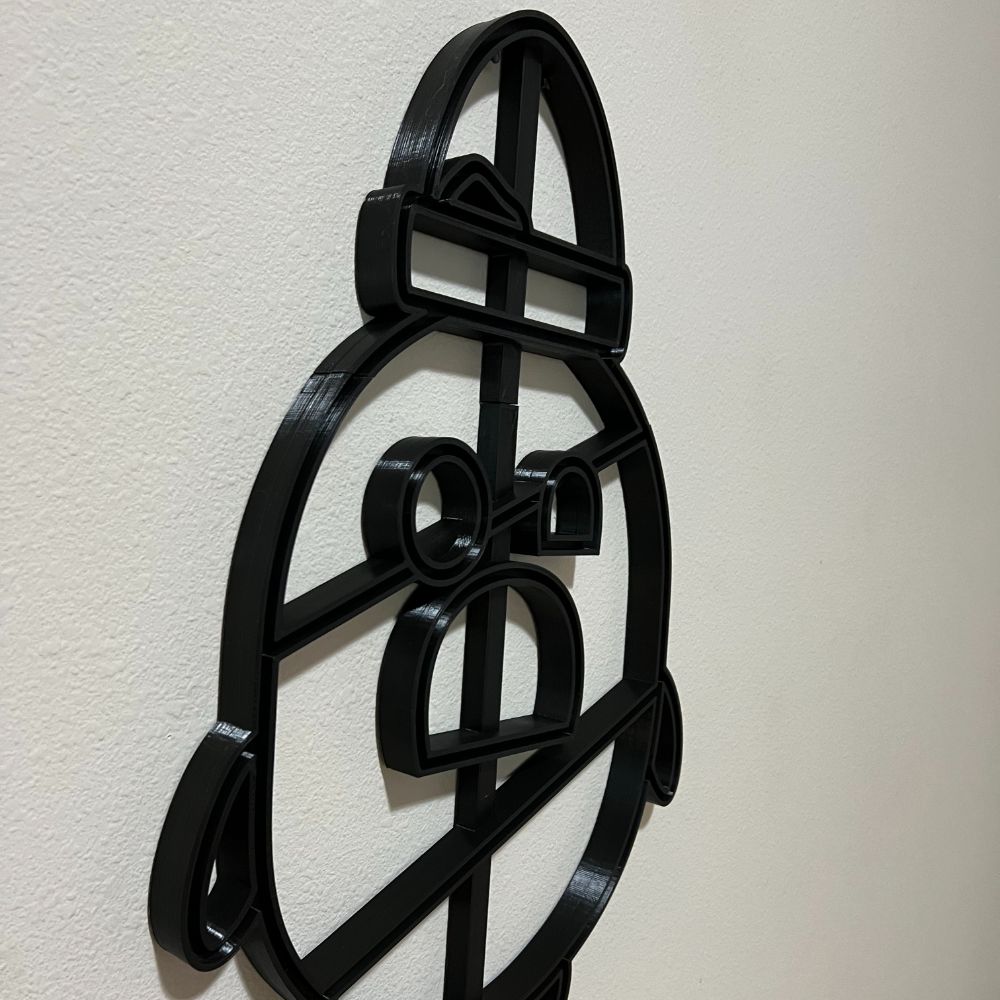
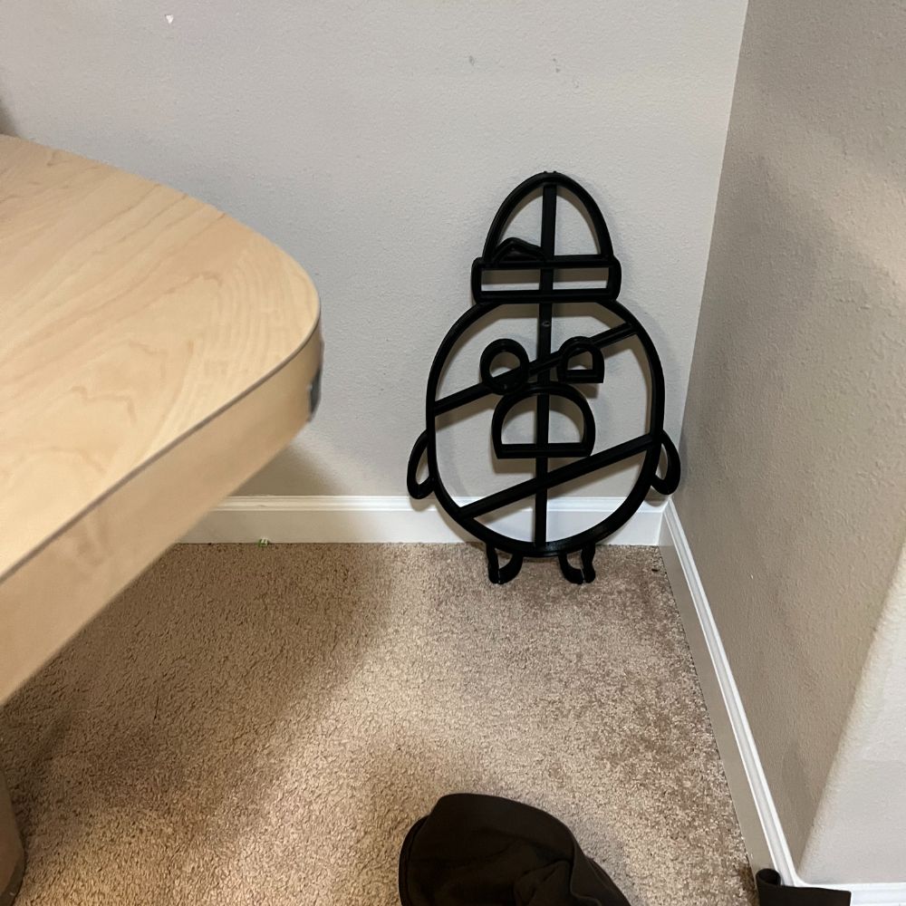
Also commissioned a logo, filed a DBA, ordered 50 boxes on U-Line for shipping. Got some Aliexpress quotes for the more expensive materials. Reserved the etsy store name and the instagram handle. Issued a few invoices. Angel made a huge spreadsheet for tracking everything as well. Will be going public fairly soon. Shipped Itvlo the Noise Toaster, so now I have to make another one.
I also found out somebody else already has a store called neon vision, here’s their website:
https://neonvision.co/


Export
2.3 – Eber-Moll model applied to basic transistor circuits
2.3.1 – Improved transistor model: transconductance amplifier
Notes
For many applications, there is no need for an advanced model of the BJT
Switch, Current Source, Follower, Amplifier
Now it is time to dive deeper
The previous model of the BJT was as a current controlled current source
That is, current in, current out
Ic = B*Ib, to be specific
Input, Ib, Output, Ic
Now we’re looking at it as a transconductance device:
Voltage in, current out
Ic as a function of Vbe
The applications for this more specific modeling include
differential amplifiers
logarithmic converters
temperature compensation
etc
all fancy higher precision analog stuff
NEW RULE #4
When rules 1-3 are obeyed, the following relationships are true:
Vt = kT/q
Ic = Is(T) * [e^(Vbe/Vt) – 1]
Vbe = Vt * ln[ (Ic/Is(T)) + 1]
notes
The current passing through the collector
Is a scaled version of Is(T)
Is(T) is the saturation current, which varies from transistor to transistor, and also varies by temperature
the scale factor is e raised to the power of the ratio of the base emitter voltage to the ambient thermal voltage
Thermal voltage is the ambient voltage present in the transistor at a given temperature, and Vbe gets ratio’d by that in order to determine how much current passes through
Vt – Thermal Voltage
q – electron charge constant
1.60×10^-19 C
k – Boltzmann’s constant
1.38×10^-23 J/K
T – absolute temperature
K
Old Rule #4 (pre-Ebermolls)
If 1-3 are followed
Ic is proportional to Ib
Ic = B*Ib
B is Beta which is h_fe
“h parameter transistor model” is no longer popular
New Rules
NPN Rules (reverse for PNP)
1 – Polarity
Vc must be greater than Ve
2 – Junctions
Base->Emitter and Base->Collector act like diodes
Base->Emitter diode is usually conducting
meaning base is higher than emitter by at least one diode drop
Base->Collector diode is usually reverse biased
current can’t flow into the base from either E or C
Control current flows into B and out through E
3 – Maximum Ratings
All transistors have max values for
Ic – current flowing through collector-emitter
Ib – current flowing into base
Vce – voltage across collector-emitter
exceed them and it breaks
Other limits worth noting
Max power – Ic * Vce
Max Vbe
NEW RULE #4
When rules 1-3 are obeyed, the following relationships are true:
Vt = kT/q
Ic = Is(T) * [e^(Vbe/Vt) – 1]
Vbe = Vt * ln[ (Ic/Is(T)) + 1]
notes
The current passing through the collector
Is a scaled version of Is(T)
Is(T) is the saturation current, which varies from transistor to transistor, and also varies by temperature
the scale factor is e raised to the power of the ratio of the base emitter voltage to the ambient thermal voltage
Thermal voltage is the ambient voltage present in the transistor at a given temperature, and Vbe gets ratio’d by that in order to determine how much current passes through
Vt – Thermal Voltage
q – electron charge constant
1.60×10^-19 C
k – Boltzmann’s constant
1.38×10^-23 J/K
T – absolute temperature
K
Old Rule #4 (pre-Ebermolls)
If 1-3 are followed
Ic is proportional to Ib
Ic = B*Ib
B is Beta which is h_fe
“h parameter transistor model” is no longer popular
Vt = kT/q
Ic = Is(T) * [e^(Vbe/Vt) – 1]
Vbe = Vt * ln[ (Ic/Is(T)) + 1]
Note that in the transistor’s active region, Vbe >> Vt, and so the result of the exponential becomes high enough that the -1 can be ignored in the formula for Ic
Ic = Is(T) * e^(Vbe/Vt)
The value that determines the collector current is actually base-emitter voltage
Beta was just a rough approximation
this new formula is also accurate over a wide range of currents, nA to mA.
If you map the actual Ic vs Beta, that’s called a Gummel Plot
Typical Gummel plots look like a wide flattish hill, meaning Beta decreases at extreme ends. It’s most stable from 10^-7 to 10^-2 A
Or, 100nA to 10mA – stable beta range
2.3.2 – Consequences of the Emers-Moll model: rules of thumb for transistor design
Notes
Some simple and handy “Ratio Rules” to help calculate changes in Vbe and Ic
Ratio Rule #1 – Change in Vbe
Ic2/Ic1 = e(dVbe/Vt)
the ratio of the new current over the old current
is equal to the exponential of the change in Vbe divided by Vt
Ratio Rule #2 – Change in Ic
dVbe = Vt*ln[ Ic2/Ic1 ]
the change in base-emitter voltage
is equal to the natural log of the ratio of the new current and the old current, scaled by the thermal voltage
A – The steepness of the diode curve.
using these ratio rules, it’s easy to derive that, to 10x collector current, we only need to increase Vbe by ~60mV.
Four More Shorthands
1
10xIc -> dVbe = +60mV
2
2xIc -> dVbe = +18mV
Ic doubles every 18 mV
3
4%dIc/1mv
every mV increases Ic by 4%
4
Ic = Ic0 * e^(dVbe/.025)
dVbe in Volts
B – The small-signal impedance looking into the emitter, re, for the base held at a fixed voltage.
now to do something awful and take the derivative of one of these formulas
Vbe = Vt * ln[ (Ic/Is(T)) + 1]
we’re going to calculate the derivative of Vbe with respect to Ic
That is, if the base voltage is constant, how do Ic and Vbe influence eachother?
dVbe/dIc = will also be units of incremental Resistance, dR
actual math
by doing a u-substitution and natural log derivative, you’ll get
[Vt + 1/Is] / [(1/Is * Ic) + 1]
We can assume the +1 is irrelevant
and then we can cancel the 1/Is
We’re left with
Intrinsic Emitter Resistance – re
re = Vt/Ic
Where Vt at room temperature is usually 25mV so either
re = 0.025/Ic (Ic in Amps)
or
re = 25/Ic (Ic in mA)
Note that this formula can be inverted and instead of representing resistance it can represent conductance
gm = Ic/Vt
if in mA and mV,
gm = 40*Ic
C – The temperature dependence of Vbe.
Even though the Vbe equation scales directly with temperature,
Is(T) scales with temperature inversely, stronger than that
To the point that Vbe actually decreases with temperature overall
Handy Rules
at constant Ic, Vbe decreases 2.1mV/C
at constant Vbe, Ic increase about 9%/C
D – Early effect.
at constant Ic, Vbe varies slightly with changing Vce
dVbe = -N*dVce
N usually around .0001 to .00001 (10^-4 to 10^-5)
Ic = Ic0 * (1 + Vce/Va)
Another way to express it is in terms of Early Voltage Va
Early voltage comes from this expression
N = Vt/(Va+Vce)
which then simplifies to
N = Vt/Va
2.3.3 – The emitter follower revisited
Notes
To summarize all of the changes and finnicky interdependencies:
Formulas:
Vt = kT/q
Ic = Is(T) * [e^(Vbe/Vt) – 1]
Vbe = Vt * ln[ (Ic/Is(T)) + 1]
Ic = Is(T) * e^(Vbe/Vt)
Four More Shorthands
1
10xIc -> dVbe = +60mV
2
2xIc -> dVbe = +18mV
Ic doubles every 18 mV
3
4%dIc/1mv
every mV increases Ic by 4%
4
Ic = Ic0 * e^(dVbe/.025)
dVbe in Volts
Handy Rules
at constant Ic, Vbe decreases 2.1mV/C
at constant Vbe, Ic increase about 9%/C
Early effect
at constant Ic, Vbe varies slightly with changing Vce
dVbe = -N*dVce
N usually around .0001 to .00001 (10^-4 to 10^-5)
Ic = Ic0 * (1 + Vce/Va)
Another way to express it is in terms of Early Voltage Va
Early voltage comes from this expression
N = Vt/(Va+Vce)
which then simplifies to
N = Vt/Va
Intrinsic Emitter Resistance – re
re = Vt/Ic
Where Vt at room temperature is usually 25mV so either
re = 0.025/Ic (Ic in Amps)
or
re = 25/Ic (Ic in mA)
or
gm = Ic/Vt
if in mA and mV,
gm = 40*Ic
Summary
Vbe now determines Ic
Beta is still in play
increasing Vbe increases Ic
constant T
increasing temperature decreases Vbe
constant Ic
increasing temperature increases Ic
constant Vbe
increasing Vce decreases Vbe
constant Ic
Increasing Vce increases Ic
constant Vbe
add an intrinstic resistor in series at the emitter
re = Vt/Ic
Generally speaking, we just say re = 25 @ 1mA
re = 2.5 @ 10mA
re = 250 @ .1mA
and so on
The source impedance of the emitter node specifically (with fixed base voltage) will just be the change in Vbe wrt to the change in Ie
But since Ie ~ Ic
dVbe/dIc = re = Vt/Ic = 25/Ic
The source impedance of the emitter node specifically is re
The reason the emitter follower has sub-unity gain is because the intrinstic emitter resistance forms a voltage divider with the load, and eats up some of the voltage on the way down
Eber Molls effect on the Input and Output Impedance of the Emitter Follower
Since there is now a tiny resistor attached to the emitter, any load connected to the emitter will be forming a voltage divider between re and RL
Output/Source Impedance
2 parallel Paths to ground from the output node (unloaded)
1
through RE
2
through re, bjt, source resistance, voltage source
Meaning the overall output impedance can be expressed as
Zo = RE // [re + (1/B+1)*Rs]
Input/Load Impedance
From the input node, the signal passes through the BJT
Then through the intrinsic emitter resistance
From there, there are two paths to ground, RE and RL
So, the overall input impedance is
Zi = (B+1)*[re+(RE//RL)]
2.3.4 – The common-emitter amplifier revisited
Notes
If the common emitter amplifier has an emitter resistor
this is called “Emitter Degeneration”
Which is pretty dramatic terminology for something that just reduces the gain a little in exchange for stability
Recall that gain for the common emitter amplifier was
Gv = -Rc/Re
now we know that Re will never be zero, but will at least be re = 25mV/Ic[mA]
this means that the gain will fluctuate like crazy with output current.
If we add a large resistor to drown out the re, like 1k or 10k, the gain will obviously go down, but it will remain stable for a larger range of currents
So as long as there’s the external emitter resistor present, we can usually just ignore re
There is another case though where you parallel the RE with a capacitor
Now, high frequency signals can ignore RE and go straight to ground, which means they’re concerned primarily with re.
That also means that re will form an RC filter with the RE-parallel capacitor
If we have a common emitter amplifier, without an emitter resistor, we will not have infinite gain
Similarly, if we measure the input impedance, we know that it’s not zero now, because that tiny re is there.
Zin is now going to be (B+1)*re
“common emitter” and “grounded emitter” are sometimes used interchangeably, to refer to when there’s no external emitter resistor. RE = 0
the “common” means ground. more specifically. the input and output share the same ground
base and emitter, share the same ground
and they both have a path to ground
the collector, no path to ground
A – Shortcomings of the single-stage grounded emitter amplifier
1. Nonlinearity
Simple 10k Collector resistor, no emitter resistor
Gv = -Rc/Re
Re = re = 25/Ic
Gain varies from -800 down to zero between 2mA and 0mA
Awful performance
Poor linearity, tons of distortion
This thing could be useful with some feedback
Without feedback, it’s only useful for small signal swings around the Q point
ONE MORE TIME
The emitter degenerated common emitter amplifier
Adds Re >> re
Such that the gain becomes effectively independent of Ic
Incremental Gain & Distortion & Nonlinearity
Several new concepts here on the grounded emitter amplifier
First
Incremental Gain
The quiescent gain is
Gv = -Rc/(25/Ic_q)
Where Ic_q is the quiescent current
Flipping this around we get
Gv = -Rc*Ic_q/25
the 25 is Thermal Voltage, Vt
and Rc*Ic is just Vrc – the voltage drop across the collector resistor
In this case, we’re specifically talking about the quiescent voltage drop
Obviously, the voltage drop across the collector resistor will change with collector current, etc.
Gv = -Vrcq/Vt
Now we can say that the gain is equal to the ratio of the voltage drop across the collector resistor, to the thermal voltage
Now, for incremental gain
Since Vrc is variable, we can say this is a function
Gv(Vrc) = -Vrc/Vt
and so the incremental gain dGv is determined per volt of dVrc and the 1/Vt factor
dGv = -dVrc/Vt
Nonlinearity
Nonlinearity can be quantified as the fractional change of gain with swing
fractional change of gain referring to gain increasing by 10% or something proportional like that
These changes in gain are proportional, so they’re referenced back to the quiescent Gain, so
(Ginst – Gq)/Gq
and swing referring to the distance between an instanteous voltage and the quiescent voltage
Since after all, signals push voltages up and down and move it away from the quiescent point. This distance from Vq is referred to as swing.
Specifically, instantaneous swing
But it’s not just the raw voltage difference, it’s also fractional, referred back to the quiescent voltage drop
That is, swing is (Vinst-Vq)/Vq
Also expressed as dVout/Vdrop in the book
Putting this together, we get our expression for nonlinearity:
dG/G = dVout/Vq
Distortion
Finally, distortion
If distortion is present, that means the signal is not perfectly linear
A perfectly linear signal has no distortion
Therefore, the measure of distortion is to take the waveform, subtract the strictly linear part, and whatever is left is the distortion
the amplitude of whatever is left is the quantity of distortion, and we measure that as a fraction of the total amplitude of the waveform.
Meaning we might get numbers like 5% distortion
For some reason I do not understand, we divide the number by 3 and say that’s the distortion
so 1.66% distortion if you calculate 5
It’s important to be clear, nonlinearity and distortion are two different ways of talking about the same thing in this context.
That is, to calculate distortion, just solve the dG/G from earlier
If gain moves from 200 to 204, you can calculate distortion right then and there
(204-200)/200 = 4/200 = 2%
2/3 = 0.7
0.7%
Even adding just a 225R resistor to the emitter will drastically improve linearity.
It comes at the price of reducing quiescent gain by 10x though
Example, given a fluctuating triangle input, you can calculate gain
use the input voltage, and our rule of thumb of +4% IC per 1 mV+
IC Changes, the voltage drop across Rc changes, and from there gain can be calculated
a simple 10V supply, 5V output bias, 5k resistor circuit being fed a 25mV triangle wave is going to have its gain flying all over the place
>20% distortion and such
2. Input Impedance
Because the signal source impedance and the amplifier’s input impedance form a voltage divider, the grounded emitter amplifier will experience further nonlinearity
if the emitter is directly grounded, then
Zin = B*re = B*25/Ic
3. Biasing
You might think you can use the eber molls equation to bias the grounded CE amp (GCEA) to some fine tuned Vbe,
But since Vbe is roughly proportional to 1/T, that means even small changes in temperature will cause the transistor to saturate.
fixed Vbe, Ic rises 10x for a 30C temperature rise
Vbe: 2.1mV/C
Ic: 9%/C
Ic: 10x / 30C
B – Emitter resistor as feedback
The transistor is a TRANSCONDUCTANCE DEVICE
Gain is in terms of A/V
Input is a voltage, output is a current
Input into the amplifier is Vin, measured from Ground
AKA Vb
Output is collector current Ic
We convert this current back into a voltage using a Transresistance device, a resistor
it converts current into voltage, and then we measure the voltage and back-calculate the current using the gain of the transresistance device (resistance of the resistor, measured in Volts/Amp)
Negative Feedback involves taking some portion of the output and feeding it back into the input
It costs some gain to have but improves many characteristics like linearity
adding an emitter resistor is a form of negative feedback
Input is VB, but that’s not what fully determines IC
What fully determined IC is VBE
Which is VB – VE
This means the input is modified, it’s subtracted by some term VE
But VE is not a static value
VE actually changes according to the output, IC – making it a sample of the output
What’s more, the emitter resistor actually serves the same tranresistance conversion role as the collector resistor.
The collector resistor converts the output current into an output voltage that’s easier to measure and pass around
the emitter resistor converts the output current back into a voltage so that that sampled voltage can then be subtracted from the input, VB in the form of negative feedback.
The circuit diagram may not show a complete loop being formed but negative feedback is present in this circuit, since a portion of the output is fed back into the input.
2.3.5 – Biasing the common-emitter amplifier – B Start
Notes
If you need high gain and so don’t want to do feedback, there are a few more options
A – Bypassed emitter resistor
Since the amplifier is meant to amplify signals, which are AC and not DC
You can just add a capacitor in parallel to the emitter resistor and then bypass it
the capacitor’s impedance decreases with frequency, so its presence means AC circuits pass through the intrinstic emitter resistance, and then have a free short to ground and can freely ignore the emitter resistor
DC can’t ignore that capacitor and has to go through the emitter resistor
This is useful, because we can have a small emitter resistor providing gain that is high and stable, while still allowing the actual signals to pass through unimpeded. The gain remains high because the voltage at the emitter remains above ground due to the emitter resistor.
You can’t have the emitter voltage too low. Something like 0.2 is too low, because fickle variations in Vbe will cause Ve to fluctuate in dramatic proportion to its total value.
If Vbe climbs from 0.6 to 0.625, Ve will drop 10%, and so will Ie. Not a good situation
Keeping Ve up to around 1V is sufficient for most cases
The whole system is more stable if you use two resistors and add the capacitor bypass for the second one though, forcing the current to pass through the first resistor.
This helps further stabilize Ve, while still retaining the benefits of increased gain at signal frequencies
bypassed emitter resistor means stable biasing without change in gain at signal frequencies!!
1/10th of whatever Vc is a good guideline for Ve
Note that if you’re going to add a bypassed emitter resistor structure like this,
When you go to calculate the input impedance of the amplifier, (for the RC filter formed by the input coupling capacitor and the input impedance of the rest of the amplifier)
you need to do it AT SIGNAL FREQUENCY
Meaning that emitter resistor is getting bypassed and not factored into the signal frequency level input impedance
you can also put 1 R in parallel with an RC series.
The lone R sets the DC bias point
The R in RC lets you set the signal-level gain
B – Matched biasing transistor
Sometimes, you can buy a chip that has two transistors in the same monolithic package
That is, two transistors, one stone.
This means that the transistors will always be the same temperature, and so temperature effects will be negated
I mean, obviously the normal temperature effects are still in play, like overheating it such that saturation occurs. But you don’t have to worry about one transistor getting hotter because it’s moving more power, and then its Vbe and Ic and all that start shifting around, etc.
C – Feedback at dc
You can add a voltage divider at the bases, but instead of connecting it to VCC like a normal person you can be a little freak and connect the top back to the collector
If the emitter is grounded, this means the middle of the voltage divider will for sure be 1D. BUT, if, for example, the divider ratio was 10:1, that means that 1D drops on R2, and then 10x1D drops on R1.
This forces the collector to stay up at ~11x1D with reasonable efficacy
This is cool, but the R1 resistor now serves as a path from the input to the output and so the input impedance is reduced pretty dramatically
D – Comments on biasing and gain
since Gain is
G = -Rc/Re
and the grounded emitter amplifier has just
re = 25/Ic
Why not just increase Ic so the re gets lower, and the gain goes up?
Well, if you want to increase the gain but keep your quiescent voltage
the higher current means you’re going to have to use a smaller resistor for Rc in order to maintain the same voltage drop across Rc
In fact, you can prove that the Gain of a grounded emitter amplifier biased to 0.5Vcc at the collector has a Gain limit of G=20*Vcc independent of quiescent collector current
Exercise 2.16
Design a tuned common emitter amplifier stage to operate at 100kHz. Use a bypassed emitter resistor and set the quiescent current at 1.0mA. Assume Vcc = +15V and L = 1.0mH, and put a 6.2k resistor across the LC to set Q=10 to get a 10% bandpass. Use Capacitive input coupling
First, the layout of the circuit
A Common Emitter amplifier has three zones: the load at the collector, the emitter, and the biasing circuit
the load at the collector is going to consist of an RLC parallel circuit
this RLC will form a bandpass filter
the emitter is going to have a parallel R//RC for the bypassed emitter resistor
one resistor to set the DC bias at the emitter terminal/DC Gain
and an RC to set the gain for signal frequencies
the base is going to have a normal voltage divider for base voltage biasing, and then a standard input capacitor as well
Next, the sequence of approach
There are five areas that need solving
A
Use given R, L, Q, and f to solve for C in the RLC
B
Select a VE, and RE for emitter bias and DC gain
C
Select R, C, and f in the emitter-bypass to pass signal frequencies
D
Bias the base voltage divider and supply ample base current
E
Select Cin by analyzing the overall High Pass Filter formed by Cin and the Input Impedance Zin of the entire circuit
A B and C can all be done first, D has to be done after B, and E has to be done last
If you can do this problem quickly and accurately, you have a good grasp of what’s going on
2.3.6 – An aside: the perfect transistor
2.3.7 – Current mirrors
Notes
A current mirror is easy to make
But you do need a matched transistor
Thankfully, in the world of ICs, matched transistors in single monolithic packages are plentiful
Here’s what you do.
Take a transistor, PNP example
Connect VCC to emitter on top
Connect Resistor through Collector down to ground
Connect Base to Collector
Now base current flows in through E->B, creates voltage drop 1D
Now Base and Collector are both VCC-1D
voltage goes through resistor and makes current IP = VCC-1D/RP
By selecting R we select the current
Now, since we have a matched transistor, and their properties are identical at all times, any Vbe we apply to the second transistor will result in an identical Ic on the other side, Thanks Eber-Molls
So we just connect the Base-Collector node to the base of the other matched transistor
Now all that’s left is to connect a load for the current source to source current through, on the other side.
If we need to change the current, we just change the programming resistor
the second transistor doesn’t get a say in the current, it just samples the Vbe of the leader.
Note, resistor goes on the opposite side of the B-E junction, always on the collector
E straight to supply rail
A – Current-mirror limitations due to the Early effect
Now, we know the VCE for Q1 in the current mirror circuit is just going to be VCC down to 1D.
In this case, 15 -> 0.6V = 14.4V is the VCE for Q1
However, the VCE for Q2 won’t necessarily be the same
Because the current is set, a wide range of load resistances can be selected and the current source will be compliant
But since V = IR, the load resistance and the output current together form the collector voltage, which won’t necessarily be 0.6V.
This means that VCE is liable and almost guaranteed to be different from the VCE in Q1
And we know from the Early Effect that VBE to maintain a fixed current actually changes dependent on VCE
Meaning the currents won’t be exactly equal, but that level of precision is not needed
You can improve the performance of this by adding matching emitter resistors that drop a few 10ths of a Volt or 1V. This negates the effects of small variations of Vbe and Vce on the output current
`
If you pay close attention
In NPN BJTs, the base current flows into the base, and combines with the collector and the sum moves out through the emitter
in PNPs, the emitter points inwards, and contains the sum of currents
Once it enters the emitter, the base current forks off and flows OUT through the base terminal
Where does this base current go?
In the current mirror, the two PNP transistors have their bases connected. Obviously these two base currents don’t just combine and cancel out. They would cease to flow and be currents in that event.
The connection that ties the two bases down to the Q1 collector will be where the two base currents flow out through
meaning, the current seen by the Rp programming resistor is actually higher than the collector current
It’s actually Ic + 2xIb
The load resistor is Ic + 0xIb, so the currents are not equal both due to early effect and due to the base current error
The wilson mirror is a clever solve for this
After the two base currents recombine, just add another transistor before the load resistor, a PNP. This PNP will take one of the base currents from the entrance at the emitter and pass it out through it’s base back over to the top of the programming resistor.
Now the programming resistor is seeing Ic + 1xIb
The current leaving this Q3 new transistor will still have one of the two Ib’s with it, so leaving the collector of the Q3 and entering the load resistor is also Ic + 1xIb
Thus, the base current error is exactly cancelled!
Hooray!
Note that Q1 and Q2 have to be matched, but Q3 doesn’t have to be part of the matching group
WIDLAR – Learn his name
He came up with a trick to unbalance the emitter resistors
The emitter resistors stabilize the voltage, but if you make them not the same value
Then the output currents will also correspond to the ratio of the resistor values
To get this correctly though, you need to account for the Change in Vbe for the new current
Thankfully the Eber Molls Equation makes quick work of this
dVbe = kT/q * ln(Ic2/Ic1)
So the ratio of the currents desired will result in a particular shift in Vbe
the ratio of the currents is approximately the ratio of the resistors
2.3.8 – Differential amplifiers
Notes
A differential amplifier does not amplify a signal
It takes two signals and subtracts them, and then amplifies that difference value
The theoretical ideal differential amplifier then, is one whose output is 100% completely independent of the individual input signals’ levels. It is purely a function of their difference.
In the real world, things aren’t so clean, obviously.
Differential amplifiers need to be understood.
They are universally used in operational amplifiers, which is Chapter 4
An essential building block.
Nomenclature
COMMON MODE
When both inputs change levels together
NORMAL MODE
A differential change in the inputs
CMMR
Common Mode Rejection Ratio
Performance characteristic of a differential amplifier
Specified in dB
Common Mode Input Range
The voltage level over which the inputs may vary
CMMR
Common Mode Rejection Ratio
It is a ratio
The two numbers are
The differential amplifier’s response to a
1. Normal Mode Signal
and
2. Common Mode Signal
Since it’s a differential amplifier, we ideally want the Common Mode amplification to be 0
and for the Normal mode amplification to be as high as we can get it
Thus,
CMMR = NormalMode/CommonMode
The Normal mode (differential response) should be much stronger than the common mode response. The ratio should be orders of tens and more
The differential amplifier is a device that converts a difference signal into a single ended signal
A difference signal is not measured to ground. It’s reference point is also a varying signal
A single ended signal is referenced to ground. It’s reference point is the zero point of the circuit.
by converting a difference signal to a single ended signal, other things like followers and current sources can make use of this signal.
If you WANT a differential signal as an output, you just measure between BOTH collectors in the circuit, rather than just the output collector to ground.
The structure of the differential amplifier can be described as follows
two NPN transistors, who’s emitter resistors both meet at a common node, which then has an additional resistors to GND or -VEE. This common emitter node is called A
The collectors have simple resistors connected up to +VCC.
There are two inputs, (+) and (-), directly at the base of each transistor.
The output is the collector over the (-) negative input.
This Single-Ended Output is the most common configuration.
This basically acts like two common emitter amplifiers that are connected at the bottom
The gain is going to be some variation of the original Gv = -Rc/Re
However, we need to calculate two gains
The Differential Gain, which is the amplification of a difference between the signals
and The Common Mode Gain, which is the amplification of identical signals
For the differential gain, we assume a SYMMETRICAL differential input signal
Meaning, the input goes up by some Vin at the + input and goes down by the exact same amount at the – input
The Vbe will stay about the same, but the actual set point of the Emitter Voltage will increase for the + input and thus the current through Re+ will increase
The Emitter Voltage will decrease and current will decrease for the – voltage symmetrically
These two effects cancel out and common point A will actually remain the exact same voltage, carrying the same net/sum current down to -VEE as the input signals vary
That is, as long as both transistors remain in the Active Region
The Gain is then that of a normal CE amplifier, but with the input change being 2x the wiggle, since this is a differential gain and the inputs changed by the same amount in opposite directions: 2xVin
Gv = Vo/Vi
Gv = Vo/2xVi
G_Diff = Rc/(2*(re+Re))
Common Mode Gain
When both signals are identical on both inputs
The rise in input voltage will cause an increase in emitter voltage on both ends
This increase in emitter voltage results in a mutual increase in emitter current that then sums together at A and through the R1 resistor
Meaning the Gain is
G_CM = -Rc/(2*R1+Re)
Note: re is still small, around 25Ohms (25/Ic)
Note: Re is small, usually around 100 Ohms or less. Sometimes omitted
Note: Differential gains of a few hundred are common
Note: R1 is usually a few thousand ohms, meaning both Re and re can be ignored sometimes
Now, putting together the Differential Gain and the Common Gain
We can ratio them and put together the CMMR
G_Diff = Rc/(2*(re+Re))
G_CM = -Rc/(2*R1+Re)
Putting these together, as CMMR = G_diff/G_CM
Cancel out the Rcs, flip the fractions
Then, see that 2R1 + Re =~ 2R1
because 2R1 >>> Re
CMMR = R1/(Re+re)
!!!
Pretty easy
As usual, we bias the collector terminal to 0.5VCC
We pick the common resistor R1 to pass around 200uA
Thus, the Collector resistor should be passing around 100uA on each dside, when the differential signal is zero
If you’re only taking one output, the other non-output transistor doesn’t need a collector resistor
Since this is still a CE amplifier, you can lower Re to raise the gain, but that will dramatically reduce the differential input impedance as well
Also similar, Re reduces gain in exchange for better linearity
We proved earlier that the max gain of a CE amp biased to 0.5VCC is 20xVCC. Differential amplifier max gain at the same bias will be half that
Exercise 2.18
Idk what they mean by Rout
is that R1 going down to -VEE or is it RC down to Q1C? who knows
whatever
assigning both to be 10k, and biasing the Collector to 2.5V (half of VCC)
we get 0.25 mA from both sides
or 0.5mA going through the 10k at the bottom
this places node A conveniently at 0V
All we need now is the Gain
G_diff = Rc/(2x[re+Re])
we know Rc, because we picked it
we know G_diff, because it’s called to be 25
we know re, because we already found Ic (re=100)
Thus, Re should be 100R
A – Biasing with a current source
push a voltage wiggle through a resistor and you get a v/r sized current wiggle
therefore, if you push a voltage wiggle through something and get an extremely small current wiggle, then you probably have an extremely larger resistor
a current source is a thingy that can take a voltage wiggle in and put out an extremely small corresponding current wiggle
you know, because it’s supposed to be a regulated current source that stays the same over some input voltage compliance range
therefore, if we can replace the R1 resistor with a current source of equivalent flow, then we should be able to artificially increase R1 by a tremendous amount
this is good for reducing common mode gain, which is the one we want low
recall G_diff is not dependent on R1
recall G_comm is -Rc/(2*R1+Re)
So if we increase R1 a lot it’ll snuff out common mode gain and increase over all CMMR
in this case we’ll use a current source biased by a zener, with the zener receiving its tax current and bias from a resistor connected to ground
with something like this, the input voltage is bounded on the low end by the saturation of the current source transistor,
and bounded on the high end by the fact that the two differential transistors always need to be supplying AT LEAST enough current to comply with the current source
as before, these amplifiers, if capacitively coupled, still need a dc bias path to ground at the base
also as before, reverse breakdown for the BE junction is 6V
the emitter resistors in the differential amplifier help mitigate this destructive current but the transistors will still be degraded if reverse conduction occurs
I’m not going to try and pretend I have any idea how to explain this evil bit hack PTAT shit
B – Use in single-ended dc amplifiers
If you have a single ended signal and are stuck with a differential amplifier, you’re in luck
in fact differential amplifiers can be configured to work with single ended signals and are actually better than the single ended amplifiers we learned about already
just ground one of the inputs (the inverting one to be specific)
and then strap in the input signal on the noninverting input
now temperature changes cause changes in Vbe that effect the output of the classic amplifier
but with the differential amplifier, the output is proportional to the difference between the two inputs.
One of the inputs is grounded, but that transistor is still working and pushing current
when temperature causes the Vbe to shift
because both transistors are matched, their Vbes shift together
and thus the DIFFERENCE between the signal input and the grounded input, remains the same.
The temperature effect is automatically compensated for in the single ended differential amplifier
Changes in Vbe are not amplified by Gdiff, only Gcomm
Also, since the changes in Vbe are cancelled out, the output wrt the input does not have the 1D dc drop we’re using to dealing with
FYI: matched transistors have drift values for their Vbe separating due to imperfect matching
an extremely good value is 0.16uV/C
C – Current-mirror active load
Take a differential amplifier and replace the collector resistors with a current mirror
G_Diff = Rc/(2*(re+Re))
G_CM = -Rc/(2*R1+Re)
Now that Rc is a current source, the gain goes up tremendously
D – Differential amplifiers as phase splitters
If you take a differential output by measuring both collectors, you get a differential signal that can be passed to a second differential amplifier
the reason you do this is to get even MORE common mode rejection
E – Differential amplifiers as comparators
A comparator tells you which of two inputs are higher
the differential amplifier is the basis of this
however, the comparator is discrete and ignores the active region of the transistors
thus, one of the two transistors is cut off at any given time in a comparator
2.4 – Some amplifier building blocks
2.4.1 – Push-pull output stages
Notes
npn emitter followers cannot SINK current
pnp emitter followers cannot SOURCE current
So if you have something like an audio amplifier powered by split supplies
You’re going to have issues, since the npn follower needs its output at 0V.
if the output goes up, towards VCC say +15V, then the transistor Vce gets to drop, because E went up
but on the other end of that signal, when e goes down to -15V, the transistor needs to Vce 30V
having one transistor do such heavy lifting to compensate for the fact it’s only supposed to be conducting for half the waveform results in tremendous power dissipation/waste/inefficiency
Class-A Amplifier- Transistor always in Conduction
Class-B Amplifier- Half Conduction, meaning you need 2 transistors
Class-AB Amplifier- Each transistor has >180 conduction, there’s overlap
Class A amplifiers are extremely inefficient energy wise, but can be accurate/low distortion
So instead we just
take the signal and send it to the base of a npn and a pnp at the same time, and connect their emitter together as the output node
then we can take the npn, and since it drops B->E, we connect the collector to +15V
then the npn, which climbs B->E, and connect its collector to -15V
This is a PUSH PULL FOLLOWER
NPN conducts on positive swings, when the signal is above +1D
PNP conducts on negative swings, when the signal is below -1D
A – Crossover distortion in push-pull stages
Because there’s a dead zone between [-0.6, +0.6]
This is called Crossover Distortion
the waveform gets corrupted as the signal crosses over from conducting within one transistor to the other
We can get around this by providing some resistors and diodes for biasing
a resistor across a voltage drop, doesn’t create any bias points to measure an adjusted voltage
a resistor and a diode, that can be used to measure 1D below VCC or 1D above ground
A diode in between two [equal] resistors can be used to measure half a diode above and below VCC’s midpoint
but TWO diodes sandwiched between two resistors creates 3 bias points,
one 1D above middle
one 1D below middle
one at middle
Now we can use the RDDR bias structure as a bias for the Push Pull follower, and then pass the signal in through the middle bias point
NOW the push pull follower has little to no crossover distortion/deadzone
before, it only conducted positive above 0.6 and negative below -0.6
But the diodes push up and pull down the signal on its way to the respective NPN and PNP and cancel out the offset
so now they just run Above 0 and Below 0
B – Thermal stability in class-B push-pull amplifiers
This is a Class B amplifier, and it’s great, but it’s not thermally stable
If Temperature goes up, the Vbe for a given Ic goes down
So the transistors in any state will heat up, either active or quiescent, relative to the diodes
this causes the current to run higher and then the transistors dissipate more heat and the Vbe sinks even lower
Thermal runaway occurs, which is not beneficial
We can get around this by making the 2D gap bigger
If we add a third Diode to the stack, and then put 2 symmetrical resistors at the emitters
Now, whenever the transistors heat up, the Vbe goes down and current goes up
But because the Vbe of the two transistors AND the emitter resistors have to add up to 3D,
The Vbe drop is compensated by the Vr rise due to increased collector current
This mitigates the thermal runaway effect very strongly
Replacing the third diode in the biasing circuit with an adjutable resistor allows you to adjust the quiescent current, the amount of overlap in conduction for the two transistors.
More quiescent current, more overlap, less crossover distortion
so now there are efficiency/accuracy tradeoffs
Also note that the signal can be coupled in pretty much anywhere
Also note that the amount of power going into the emitter resistors will be fairly high, and their resistance will be fairly low (<10R)
C – “Class D” amplifiers
Class A, AB, and B amplifiers are all linear stage amplifiers – they still output some linear signal
Class D amplifiers do not have a linear output, they use rapid switching schemes
You just need to switch the Push Pull on and off extremely quickly, 10x faster than signal frequency
eg. 250kHz switching for a 20kHz audio signal
Because the switches are never ACTIVE and always CUTOFF or SATURATED
ACTIVE
CUTOFF
~0 Ic
SATURATED
~0 Vce
There is very little energy waste in class D amplifiers
They do require some Low pass filtering afterwards though to smooth out the very high frequency chopping signal
2.4.2 – Darlington connection
Notes
A Darlington connection is the double transistor wombo combo you’ve been waiting for
Just take the amplified output current of one NPN and feed it directly into the base of another NPN
This does work, and it’s called a Darlington Connection
Some consequences include
overall Beta = B1 x B2
overall Vbe = 2 x Vbe
Q2 is slow to turn off, since it just needs Ib, but is receiving Ib+Ic into its base.
If Q1 turns off, the output current will drop, but not instantaneously, and so it takes a while for the Q1 output current to drop to a level where Q2 can no longer conduct.
Sure this all happens extremely fast from our perspective, but it’s important to know that Q1 and Q2 do not turn off at the same time
One way to improve this circuit is to add a resistor between Q2’s B and E
This may seem redundant, as you circumvent the second transistor, but there are distinct advantages.
First, all transistors have leakage current, and this provides the Q1 leakage current a path to ground. Without it, there are some circumstances where the leakage current could activate Q2
As long as the leakage current * R is less than 1D drop, Q2 won’t turn on
Second, this stabilizes the overall Vbe of the pair as well as the collector current of Q1 (again, by providing a guaranteed path to ground)
When Q2 is on, the voltage drop across the resistor is maxed out at 1D.
It won’t go higher than that, because that would require Vbe to go up to incredible numbers as well
Since Q1 now has a reliable path to ground, the base current previously being forced down Q2B’s throat can now relieve itself through the resistor. Q2 turns off faster
A – Sziklai connection
like the darlington, but generally preferred by designers
since it uses a PNP and an NPN both, there’s only 1 Vbe
Since the PNP receives it’s current from VCC and passes through the base
Q1 being on gives that base current a path to ground, turning on Q2
if Q1 turns off, that base current has nowhere to go
This is why it’s advised to add a Q2 B-E resistor, for all the same reasons as in the darlington
Note that this does create a simple voltage divider between VCC and Ground now that there are two resistors in series, with some transistors dancing around them
It still has B1xB2 but the one Vbe is more predictable and consistent
Note that since the combination acts as a single transistor with its own collector, base, and emitter
The minimum saturation voltage of the Sziklai Equivalent Transistor is 1D
If Q1 is on, Q2 is on – general rule of operation here
If Q1 is saturated, Q2 is definitely on
If Q1 is saturated, Q2 is on, and the R1 voltage is 1D
meaning, Q1 has near zero Vce, yet its collector is 1D lower than VCC
So the emitter of Q1, and the Sziklai combo will be 1D lower than VCC
Thus, the saturation of the sziklai cannot drop below 1 Vbe
BIG CIRCUIT BREAKDOWN!
Replace input node with an input transistor that also sinks current, with the top resistor being Rc for setting that current
Replace the diodes with a triple parallel – one resistor, one pot to adjust the bias, and then a branch with an NPN tapped off of that bias, and then a third branch with a capacitor so signals can bypass all this.
Then replace the Push Pull transistors with PNP and NPN Sziklai Transistor Structures
Keep the shared emitter resistors for thermal and Vbe stabilization
Then There seems to be some sort of feedback/stabilization capacitor that hasn’t been covered yet
B – Superbeta transistor
superbeta transistors are not to be confused with sziklai and darlington
Superbeta transistors are MANUFACTURED using special techniques
sziklai and darlington are TOPOLOGIES
2.4.3 – Bootstrapping
STOPPED ON PAGE 112
2.4.4 – Current sharing in paralleled BJTs
2.4.5 – Capacitance and Miller effect
A – Junction and circuit capacitance
B – Miller effect
2.4.6 – Field-effect transistors