
1/31/2022 – 2/13/2022
Summary: My goal for these two weeks was to wrap up calibration on the printer, and then start learning LTSpice and KiCAD. I wound up replacing some parts on the 3D printer and having to adjust temperature and retraction settings after some test prints, since I was having some sticking issues. As for the CAD programs, I spent a full week learning the ropes around LTSpice. Once I was feeling pretty confident, I started building out the Analog Synth from my reference book. This exercise took on a life of its own as a parallel project and I put most of my hours this week working on the Synth. I learned a lot about debugging and troubleshooting simulations within LTSpice. Towards the end of the period, I moved onto KiCAD. At this point, I’ve already taught myself FreeCAD and LTSpice in a short time, so KiCAD was pretty easy to pick up, despite being the complex, menu and library wise. I didn’t quite have the time to finish the KiCAD tutorial series due to prior obligations, so the first order of business for D will be to finish the tutorials and order the first PCB. After that, it’s power supply design series and laying out a board for the Synth.
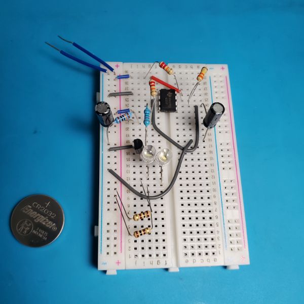
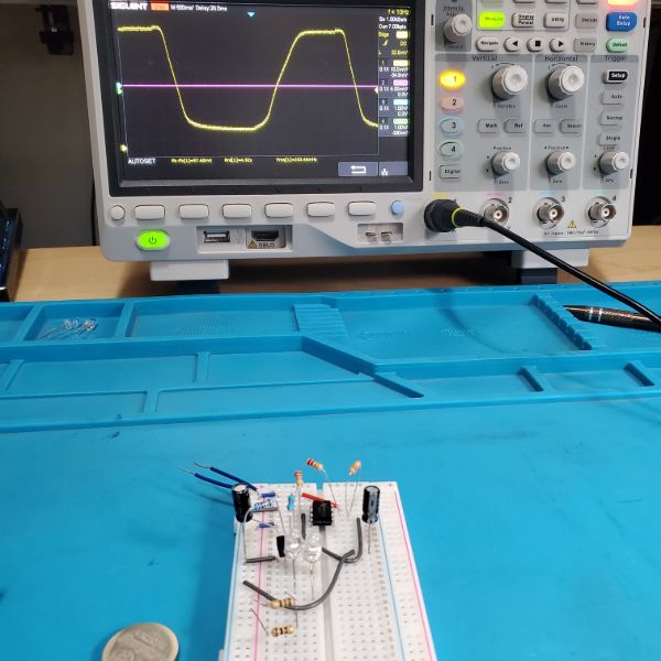
The synth gave me a huge amount of trouble and became a great learning experience. I’ve built complicated circuits on breadboards before without using simulation tools and now I feel like a fool for not learning how to use them sooner. I can test changes and measure them about 10-20x faster than I could by swapping parts out on a breadboard. I still had some issues reproducing exact results in terms of actual waveforms when it came to building the 555 Badge.
I was getting frustrated because the Synth seems to stonewall me no matter how I try to analyze or construct it, whether on breadboard or on KiCAD or on LTSpice, or just trying to analyze it in my head reading the descriptions the author wrote. But I decided to persevere and I eventually honed in on the reason the simulation kept crashing. The JFET responsible for creating the ramp wave in the VCO circuit was the issue. Something about the exponential voltage to current conversion relationship on that JFET lagged the simulator a severe extent.
It got to the point where I had to be creative and slowly figure out which set of conditions are most stable for the simulation through trial and error. Then I tested other features like AREG and LFO mod depth on the VCO separately before moving on with the most stable state. Eventually I was able to run the entire synth, all 9 modules at once for at least 2 seconds before the sim crashed, which gave me all the info I needed to know that I had built it correctly.
On top of learning hands-on how to troubleshoot in LTSpice, I also have a significantly deeper understanding of how the synth is constructed, including the clever use of opamps, resistors, transistors, and capacitors to create the type of waveforms that can be used together constructively to form a synthesizer. It’s actually really cool and I’m glad I took the time to keep pushing.
Once I was satisfied with the LTSpice files, I backed them up, exported the schematics, took some pictures, and got ready to move onto KiCAD.
KiCAD is a little frustrating because there’s so much library linking between symbols, symbol creation, footprints, footprint creation, and the actual circuit schematic/layout, and then of course, the actual specs and design rules of the PCB at the end.
Moving into D, I’m looking to develop more expertise with KiCAD and the board layout by using the Synth as another project to cut my teeth on. I’ll be working on that in between sessions of trying to dissect the power supply design video series. It’s pretty information dense, and it’s all brand new to me. If I can acquire a grasp over the PSU design as strong as my current grasp over the Synth design within the next 2 weeks, then there shouldn’t be any trouble keeping up with the schedule I laid out a few weeks ago.
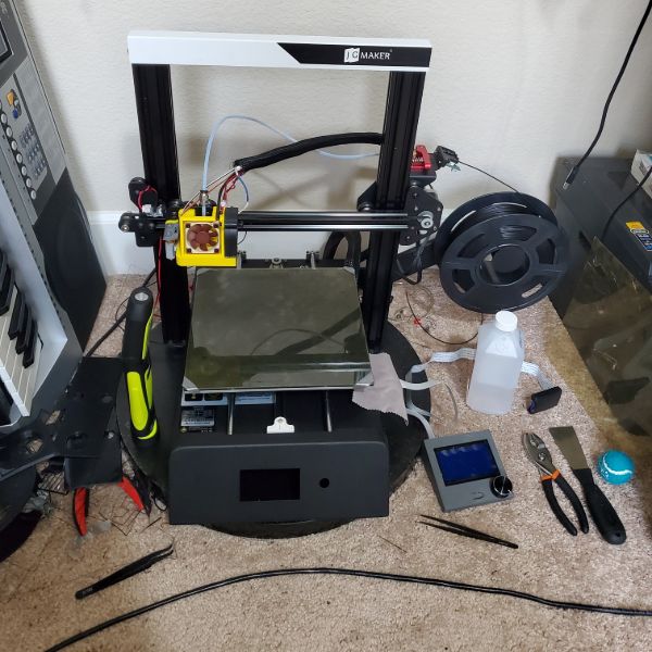
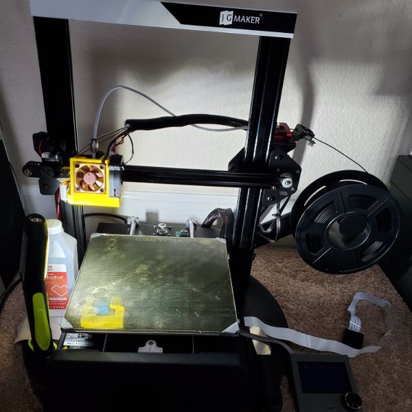
I’m still having trouble printing a specific type of vertical hexagon lattice with the printer. Some issues with retraction/z-hop. It drags into existing pillars and knocks them down, ruining the print. Other than that, it’s been working pretty great since I finished upgrading it.
Once the 555 Badge, Power Supply, and Analog Synth are all done, it should be about mid April, and then I’ll be ready to move on to more Software and HDL specific learning. I did some research into if it would be worth my time to try and write Blasteroids III in C++ as a demonstration project, but I’m still on the fence about that. I’m also trying to get to Verilog and the FPGA material sooner than later. After these three projects are closed, I’m going to run through Monty Choy’s interview question list. I’d rather spend the time scouring The Art of Electronics, but I don’t think that’s the best use of my time for now. After this 6 month stretch is complete, depending on where my personal life is at, I might shift into a deep, intensive dive into that textbook.

Cobra
Timeline
January
A
3D Printer
B
3D Printer
February
C
Power Supply
D
Power Supply
March
E
Power Supply
F
Interview Questions
April
G
Interview Questions
H
Intel/Quartus
May
I
Tutorial Sites
J
Tutorial Sites
June
K
FPGA Projects
L
FPGA Projects
Interview Questions
4 weeks
Intel FPGA
2 weeks
FPGA Projects
4 weeks
Power Supply
6 weeks
3D Printer
4 weeks
C/C++/Python
Verilog
Art of Electronics
Resources List
Monty Choy Hardware Interview Questions
1
Digital Design HQ Discord #Resource Dump
2
EEVBlog Power Supply Design Series
3
Intel FPGA Technical Trainings
3
Digikey intro to RTOS
4
Digikey intro to FPGA
4
Digikey intro to KiCad
C
EP 1 – How PCBs Are Made
https://youtu.be/vaCVh2SAZY4?list=PL3bNyZYHcRSUhUXUt51W6nKvxx2ORvUQB
Steps to the Process
Design Circuit
Create Symbols
library editor
Schematic Capture
eeschema
Create Footprints
footprint editor
Generate Netlist
cvpcb
Board Layout
pcbnew
Production
GerbView
Generate BOM
Digi-Key
EP 2 – Create a Schematic Symbol
https://youtu.be/c2niS9ZRBHo?list=PL3bNyZYHcRSUhUXUt51W6nKvxx2ORvUQB
Reference Designator
aka REFDES
list of refdes
https://en.wikipedia.org/wiki/Reference_designator
Symbol Creation Process
New Project
Edit Schematic Symbols
Make New Library to hold Symbol. Add to Project Directory
Make New Symbol
Assign Symbol to Project Library
Set Symbol name, REFDES, and properties
Add Pins
Make the Symbol
Save
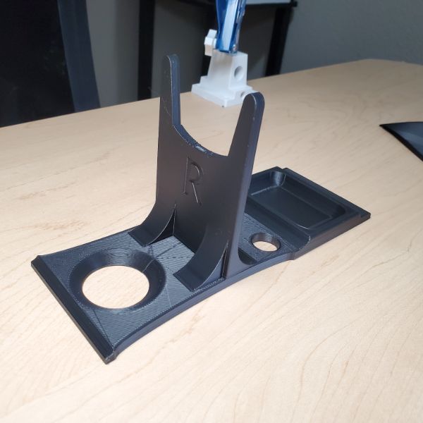
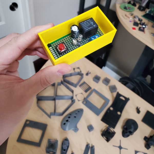
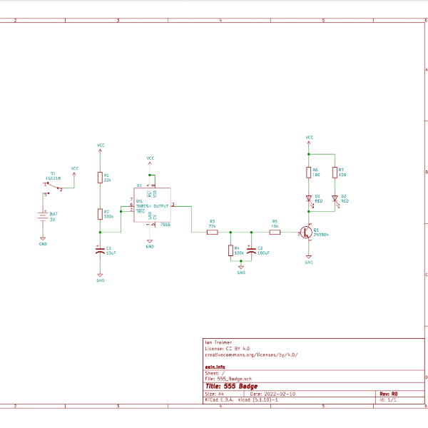
You have to create the symbol for the 555
So you open a new symbol and save it
But the symbols have to be assigned to a library
So you make a new library that’s empty, inside the project directory, so it can hold the custom symbol
But it doesn’t put the custom symbol in the empty library by default, so you have to load the library
So you go to the library manager and ADD the empty library to the main list of libraries
Right clicking overlapped elements will request a clarify selection
Shortcuts
SHIFT + ? – open the keyboard shortcut list
M to move stuff
R to rotate
Middle Click Drag to pan
Add Pins
Build out pins based on data sheet
Each pin requires a few things
Give it a name and a number, don’t worry about the cosmetics until later
Electrical Type refers to the ERC at the end. Apparently it creates trouble
In order to ACTIVE LOW and put a bar over a pin name, you have to put a ~ in front of it
Ex: ~TRIGGER
You can use the Anchor Tool to resposition the origin point of the symbol
REFDES on top, component name on bottom
File > Save Current Library
Include latest component changes, obviously
Close Library Editor
Kate Moon comment
For version 5.0 things have changed a bit:
1: Go to Tools>>Edit Schematic Symbols (Wait for Libraries to load)
2: Press Op-amp thing
3: On the Symbol Editor page go File>New Library
4: It will open a page where it wants you to choose a name. Type in 555_Badge.lib >> Save
5: Add to Library Table >> Project >> OK
6: Now you have a library that will hold the component you will make
7: Now start to create a part by going to Symbol Editor Window then click on the Op-amp thing
8: A Select Symbol Library should open and you should see your library listed: Choose 555_Badge >> OK
9: Symbol Properties >> Symbol name >> “7555” >> OK
10: It automatically makes 555_Badge your working library and you can see it on the left-hand-side project pane
EP 3 – Schematic Capture
https://youtu.be/4Gtd7xY6zS4?list=PL3bNyZYHcRSUhUXUt51W6nKvxx2ORvUQB
PCB Layout Programs are not usually helpful for Circuit Design
This is the part where you lock down exactly what the schematic is
Simulate it in LTSpice
Build it on a Breadboard
Either clean up the LTSpice Schematic or Draw out the Schematic on Paper for reference
Tools > Run eeschema to start Schematic Capture Process
To Keep track of changes and versions and titling, go to File > Page Settings
Press A to drop component, open component Chooser
Build the schematic
Make use of the “Device” Library
Mouse over a resistor, and press E to edit its data, or V to just edit the value
It’s common to change the value of the LED from LED to the color, like, Blue
C to copy component
Be sure to check datasheets for components like transistors to make sure you know the pinout for the component. And verify that the datasheet’s pinout matches the schematic symbol in KiCAD
This design uses a battery clip holder and a slide switch. These components aren’t in the default KiCAD libraries, so it’s necessary to add a custom digikey library in order to proceed
Adding Custom Libraries to KiCAD
Go to the projects folder \KiCAD\ and make a folder called \Libraries
Download the KiCAD library off of GitHub
https://github.com/Digi-Key/digikey-kicad-library
Extract zip into a folder in \KiCAD\Libraries
The library will contain two subfolders, one for footprints, and one for schematic symbols
Now add the libraries to the open project in KiCAD
Preference > Add Libraries
You can add a library to the global list, or you can add one to the local project library list. In this case, we just need to add two libraries from the digikey repository into the local project library.
Click the + symbol to create a new empty row, Click the folder icon to select a library to occupy a new row. The folder automatically creates a new row. Change between Global and Project using the tabs
Check that the libraries loaded correctly by finding them in the Add Component menu
EP 4 – Create a Footprint
https://youtu.be/ZHH4G_EWhm0?list=PL3bNyZYHcRSUhUXUt51W6nKvxx2ORvUQB
Creating a custom footprint
You might want to make the footprints when you make the schematic symbols as well
More library management hell
First, Open Footprint Editor
An example of what not to do: saving the footprint in its own new library, instead of the other new empty one you just created
You have to open a new Footprint
Then you have to make a new library,
Specificy that library as a local/project library
Save it within your project folder (\KiCAD\Projects\555_Badge\555_Badge.pretty)
Name the foot print, and save it to the library
OR
Preferences > Manage Footprint Libraries
Get to this screen again, but for managing footprint libraries instead of component symbol libraries
Make sure you know how to search components on DigiKey
IPC.org is an electronics standards committee that determines the naming conventions of PCB Footprints
https://www.cskl.de/fileadmin/csk/dokumente/produkte/pcbl/ipc_standard_pcb_library_expert_Land_Pattern_Naming_Convention.pdf
Some data sheets will be in mm, inches, both
Get comfortable with both..
DIP tend to work better with Imperial
SMT tend to work better with Metric
1 mil = 1/1000 inch
Pay attention to the unit select
You can also resize the grid
In order to figure out your footprint design, you will have to do math using the data sheet’s listed dimensions
Note that the origin point is in the center of the package, but the X+ is to the right and the Y+ is down. Using this, and the size tolerances for the package as listed on the datasheet, figure out the coordinate locations of the (8) pins and the (4) corners of the component body. You’ll also have to figure out the diameter of the pins, and then assign a drill hole that is slightly larger than that so that it can fit through, and have room for solder to bind.
Place a pad
The outer circle of copper, from the edge of the drill to the edge of the copper, is called the Annular Ring. The thickness should be about 15 mil. So double that because it’s a diameter, and then add the size of the hole (30mil) and so the total size is 0.060 inches, 60 mil
Be good in this menu
CTRL D to duplicate a pad
Once all the pins are sized, placed, and numbered properly, draw out the body
Even the lines that draw the body can be defined with precision X, Y coordinates. Be sure to take note of the thickness of the line, as well as the layer it’s on. For these body lines, use the F.Fab layer, as they will not be printed, but provide a visual reference for the fabricator
When drawing lines be mindful of which layer you’re drawing on
After creating the fabrication lines, you should also add some lines onto the silkscreen layer so that you can assemble the board without referencing any other schematics. Just draw some lines on the edges of the rectangle that don’t intersect the pins, and then put a dot next to pin 1 outside the body of the footprint. Make the silkscreen lines slightly larger.
Make sure the name of the footprint is on the Fab Layer, so it doesn’t get printed
Make sure the REF** reference designator is on the silkscreen layer. That way when the footprint is assigned to a specific component in the schematic, the footprint will automatically populate that parts refdes
Footprint complete
Note that you have access to the full digikey libraries, which means that you can reference premade footprints if you need something, or if you need to make something similar you can use a copy of a premade footprint as a starting point
EP 5 – Associate Footprints and Generate Netlist
https://youtu.be/Ghv0bGiZFL8?list=PL3bNyZYHcRSUhUXUt51W6nKvxx2ORvUQB
Basically, you’ll be pressing these buttons in order
The first one, Annotate Symbols, will automatically replace all the R? refdes with R1, R2, R3… throughout the schematic
The second one, the Ladybug, is the ERC, Electrical Rules Checker. You can run it now, but because the pins weren’t assigned dutifully at the beginning it will only yield errors. Skip this one and move onto the third one
The Third One, Schematic to PCB symbol, is the footprint assigner “CVPCB” Open this and begin assigning footprints to each component in the schematic
Yet again it is time to manage libraries
After adding the digikey footprint libraries, filter the libraries for what’s relevant to the component at hand
The first filter takes the selected component from the schematic and identifies any footprints that are for the same type of component. So if you have a capacitor selected and click this first filter, you will only get footprints for capacitors
The second filter matches for the number of pins on the selected component
The third filter filters by the library selected on the left. Clicking a library on the left section will automatically enable the third filter. In order to disable it and scan all libraries, just click the Filter-L button again to unselect.
The fourth filter is direct search
In order to double check that the footprint you’ve selected is appropriate for your needs, use the footprint viewer:
Once you’ve confirmed you want that footprint, double click the footprint on the right section in order to assign it to the selected component in the center section
You can bulk-assign by holding shift, ctrl, while selecting, and then assign a single footprint to all your resistors
The most proper way to assign footprints to resistors and capacitors and transistors and the like, is to go on Digikey, and search for a part that is appropriate, cheap, and available, and use it’s dimensional specs as a reference for selecting your footprint
This 10uF capacitor has a Lead Spacing of 0.079″ or 2.00mm
A Size/Diameter of 0.197″ or 5.00mm
So check the footprint list for a capacitor with those dimensions
Note the difference between Axial and Radial
Radial is how these tube caps work, pins on same side of a cylinder
Axial is how resistors are, pins going through a main body
So, Radial Cap, Through-Hole (THT) 2mm Pins, 5mm Diameter
Make sure the minimum qty on DigiKey is 1, or you’ll be upset
With Resistors, most 1W, 1/4W resistors are ~6mm long, and the leads can be spaced just slightly wider than that, so a footprint like this works in most cases:
Once all the footprints have been assigned, it’s time to click the Fourth Button, which is Generate Netlist
The netlist can be generated in other formats for other softwares like OrCAD, but we’re staying in KiCAD. Save the .net netlist into the project file folder
EP 6 – Place Parts and Define Outline
https://youtu.be/dM5b_s2ysVk?list=PL3bNyZYHcRSUhUXUt51W6nKvxx2ORvUQB
Showtime
First things first, edit the Page Settings with author and project and license info, just like the Schematic
Switch grid to Inches, 50 mil Grid. You’ll be switching often during board layout phase. Most board houses use Imperial.
Import Netlist
Load the netlist file, then click Update PCB. Now all the parts are laid on top of eachother. Cringe
Netlist .net file is listed on windows as a LTSpice Netlist. I wonder how I can import/export these files across KiCAD and LTSpice
It’s useful to start off by assigning some design rules for the board to ensure no parts end up too close together
For this PCB Tutorial, he’s using oshpark
https://oshpark.com/
The board house manufacturer will provide design rules for your order
https://docs.oshpark.com/design-tools/kicad/kicad-design-rules/
Open File > Board Setup
Since the board house has to keep up with the tools, their instructions on setting up board layout are actually more up to date than the tutorial video
After setting up Design Rules and Net Classes according to the boardhouse’s specs, untangle the ratsnest
Once the ratsnest is somewhat OK, define the dimensions of the board
In this case, the board is supposed to look like an ID badge, so he references ID Wholesaler .com for the most common ID Badge dimensions, which are 3.375″x2.125″
Note that the cut edge tolerance for PCBs isn’t great
Defining Board Boundaries
First, select the Edge Cuts Layer, then the Graphic Line Tool
Pick a point on the X,Y to be a pseudo-origin, such as 5,5.
Build a rectangle anchored on 5,5 at the corner.
Use the board dimensions of 3.37×2.12 and adjust the defining points of the line to create a rectangle of those dimensions
Set the line width to 1mil
http://www.555-timer-circuits.com/flashing-led.html
Built Model in LTSpice
4
FesZ intro to LTSpice
C
This guy has a crazy wealth of knowledge…
EP 1 – Getting Started
https://youtu.be/JRcyHuyb1V0?list=PLT84nve2j1g_wgGcm0Bv3K4RSl2Jdjsey
R for resistor
Left Click to Pan
You can drag wires through components to hit both terminals
Right Click Components to adjust their settings
Note that right clicking a component and right clicking a text-tag will result in different edit menus
Scroll to zoom
You can add text to the circuit to annotate what it does
Many types of Simulation, 6 total:
Transient
AC Analysis
DC Sweep
Noise
DC Transfer
DC op pnt
Mainly focusing on Transient
Measurement window notation might say V(n001) which means, the Voltage of net 001. net 001 or n001 refers to a node in the circuit
Right click a trace to open its settings and delete it from the measurement window to get the scale of the graph to adjust
This menu also allows you to edit the algebraic expression of the graph as well as the color
Once you have just the desired measurement, you can right click the black graph space and click zoom to fit to get the graph range to autoadjust so you can see the actual value
If you Left Click on the measurement’s tag, it’ll open a graph tracer that allows you to click and drag and receive X,Y coordinates that fall on that measurement’s traced line. This is a good way to receive actual, precise values
In order to measure voltage, click wires. In order to measure current, click components. I can’t screenshot it, but the cursor changes to different symbols
You can also manually change the graph’s range and scale by right clicking the range and entering values for min, max, step. including logarithmic
Net names like (n002) are automatically assigned within the circuit, but they can be manually renamed using the Net Label tool. The Net label requires you to wire in the Net Label you created into the node that you want to rename. When you rename the node, you have to re-run the simulation.
You can also plot the Power consumption of a component. Just mouse over the component as if to measure the current, and then hold ALT. This will change the cursor to a thermometer, and ALT-M1 will then add a power measurement to the graph
Note that the resulting graph line will be an automatically formed algebraic expression representing the power consumption of that component
In this case V(N001,Output)*I(R1)
You can see that the Voltage has two parameters separated by a comma, which almost definitely references a difference between those two node voltages, which would represent the voltage drop across that component, which would be necessary to calculate the power consumption of that component
Syntax: V(higher voltage, lower voltage) => (high)-(low)
Measuring the power supply will tell you how much power is needed to run the circuit, which is useful
If you want to clear away all the traces except one without having to manually delete all the traces, just double click the measurement probe and it’ll show just that one trace
In order to measure a voltage difference between two nodes without typing out an algebraic expression, just Left Click and Drag from the first node, and then release while hovering over the second node to subtract the first from the second
You can edit the simulation command by going Simulation > Edit Simulation Cmd, or by simply right clicking the text line that the simulation command creates (“.tran 1”)
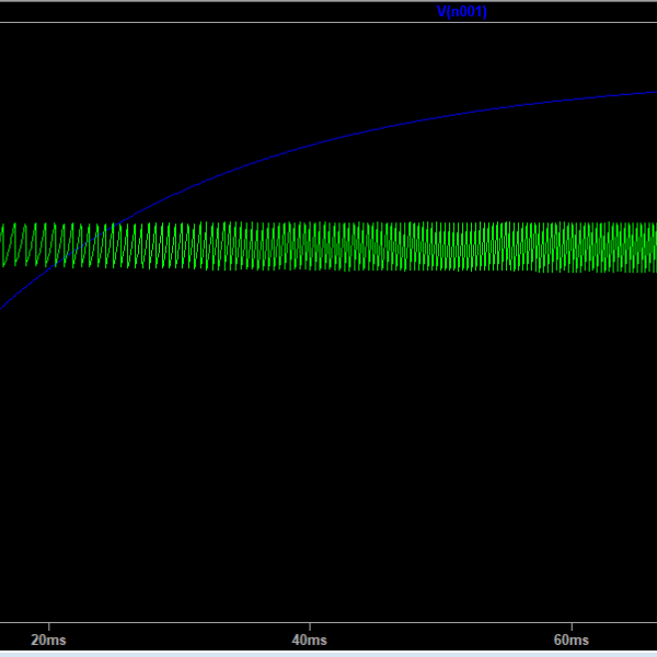
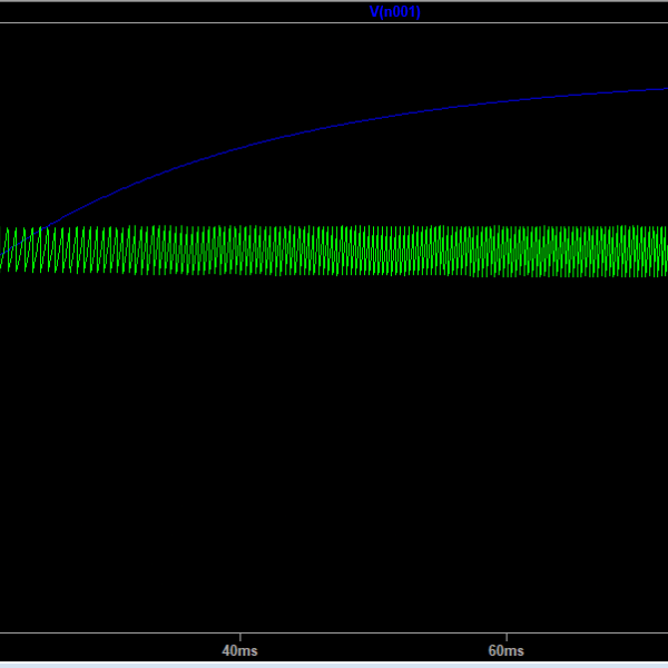
There’s a checkbox for “Start external DC supply voltages at 0V” which causes the power supply to quickly ramp up to set voltage from 0V, rather than starting at t=0 at full voltage
This is called startup in the command line, and is good for measuring the startup characteristics of the circuits
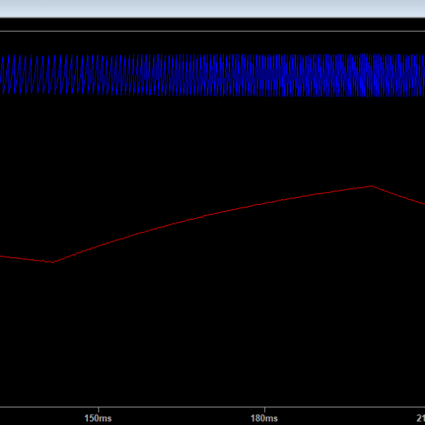
Without the capacitor connected, but with Startup still active, the result is an unsmoothed ramp. The blue line represents V(output)
You can left-click and drag a box on the black graph space to set a new range/zoom in. This is useful for startup transients
NOTE: CTRL+Z does not result in an UNDO command. It results in a zoom area command. This is not helpful. If the circuit is lost in the schematic window, just press Space to recenter the circuit.
Undo is bound to F9
Use the Cut command to Cut wires. This will also cut components, so if you want to temporarily disconnect something, be sure to cut the wire and not the component
EP 2 – AC Analysis + EP3 – .param and .step directives
https://youtu.be/P_ENvucaZkI?list=PLT84nve2j1g_wgGcm0Bv3K4RSl2Jdjsey
https://youtu.be/ARE5nwiHI0Q?list=PLT84nve2j1g_wgGcm0Bv3K4RSl2Jdjsey
Does AC steady state analysis. So no startup or shutdown. That’s what transient is for. Once DC values are stable, that’s when it injects a small signal frequency sweep
Options are Decade, Octave, Linear, and List
In order to configure a voltage source as AC instead of DC, you have to go into the Advanced options
Simple Low Pass Filter setup
After running the AC simulation, the graph will appear, with dB and Phase shift as two vertical axes, and then Frequency as the horizontal axis. There is no time axis, because this is not transient analysis, it’s frequency analysis.
In order to trace phase or magnitude, you just have to click the radio button after double clicking the name of the measured quantity to open its cursor menu
It may be useful to verify the behavior of the circuit indicated by these results, by copying the circuit into a separate schematic drafting window, and running a transient analysis on it at a particular frequency.
You can’t drag a box and select multiple components by default, but you can use the copy command to initiate a drag-box sequence. once the box is released, a copy of the components will be attached to the cursor and available for drop off in a new schematic
You can measure the sine waves by clicking and dragging a box as though you wanted to resize the graph, and checking the numbers at the bottom of the window. In this case I can see that the amplitude of the input waveform is 2V
LTSpice doesn’t have a component for potentiometer, so you have to create one using .param
1. Create a Spice Directive
2. Create a parameter named “pot1” with a value of 100k
3. Create a second parameter to tell Spice where the potientiometer is set
This process is essentially creating reference-able variables that you can use as formulas in component value fields, as long as they’re in {} curly brackets
The value R in ohms of R2 is {pot1*pot1dev/100} Ohms
pot1 = 100k, pot1dev=50, so R2={100k*50/100} = 50k Ohms
Be very careful with these formulas, it’s very easy to make a typo and overlook it and wonder why you’re in hardware hell
4. Create an AC simulation that will sweep the input signal through the audible range, 10Hz – 30kHz
5. In order to comment out directives, simply edit them and add a semicolon; to the front of the line, before the .param directive
6. Now instead of statically defining pot1dev, we can use .step to create a sweep for parameter pot1dev that ranges from 1 to 99 in steps of 10
7. Once the sweep is run, you can left click the V(output) measurement, and select between the plotted lines in cursor mode by using the up and down arrow keys
In this case, we’re looking for the most horizontal line, where the magnitude of the signal is least affected by the filter circuit. Using the up and down arrow keys to cycle between the curves until we find one that is flat on both left and right side of the frequency sweep.
Once found, we want to check what the positions are for the potentiometers. Once the curve is selected, Right Click the dotted lines forming the cursor crosshair and it will list the parameters that describe that curve:
You can choose to not plot phase by right clicking the right vertical axis
.step and .param directives are incredibly powerful
they can be used to assign and change the same value to multiple components all at once. example being a 3rd order low pass filter where all the R and C are the same
.step can also have a list style sweep
.step param var1 list 1k 10k 100k
Runs three values
.step param var2 1k 10k 1k
Runs 1-10k in steps of 1k
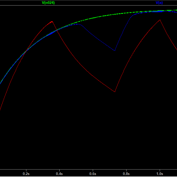
It can be very useful to plot a voltage source with a theoretical output to compare to the actual circuit simulation output:
s
Some keyboard shortcuts
R Resistor
C Capacitor
G Ground
Del Cut
F3 Wire
F9 Undo
Shift+F9 Redo
CTRL+R Rotate
F6 Duplicate
F7 Move
EP 4 – How to import libraries and component models
https://youtu.be/8V5XabccFaE?list=PLT84nve2j1g_wgGcm0Bv3K4RSl2Jdjsey
It shouldn’t matter which SPICE you’re using, all SPICE models should be cross compatible
There are three ways to import libraries and component models into LTSpice
1. Include the entire model description as a Spice Directive, just like a .step or .param operation
In this case, you take the component value field, which is D when unassigned, and rename it to match the name of the imported .model
This method will not permanently add the imported Diode to the master Diode Library:
2. Add a textfile .lib of the component to the Documents/LTSpice/lib/sub directory, and then add a Spice Directive that uses .include to include the library in the schematic
You can also include to an absolute path. The .include command does not assume filenames.
Insert the file into LTSpice/lib/sub
Once the .include is set up, there’s no need to rename the diode or reassign it’s value because it’s the same model accessed from a different method
This method still does not add to the master diode library
3. Add the .lib file’s model contents to the master library of LTSpice by editing the master diode library file and including the model data
Open Documents\LTSpiceXVII\lib\cmp to find the master libraries
Here’s what the master diode library looks like:
So, to add a new diode, just paste the model contents at the top:
This is a good time to reformat, and tweak any names or parameters before closing it off. I’m also going to add a comment that indicates there’s a section of imported models
You have to restart LTSpice in order to reload the library files after making these changes
Now the diode can be selected via the library or by typing in the part name into the value field
Importing Nonstandard Components
Some components don’t fall under the standard categories, meaning these categories
If you want to add an opamp, you can still do methods 1 and 2, and just use a universal opamp symbol, with the part name applied to it. This is actually explicitly describe in the part description
If you want to add an IC, that’s even more nonstandard. You’ll probably have to auto-generate a symbol for it.
In order to do THAT, you have to place the .lib file in the /sub folder, and then open the .lib file IN LTSpice. You may have to change file selection to all file types in order to see the files in /sub
From there, right click the component name and select create symbol
Symbol can be edited arbitrarily, but is usually good to go as is. Make sure to save it if you’re happy with it.
The symbol will be found in the AutoGenerated folder of the component tree
You can find most components have Spice models that you can download, it shouldn’t matter which one
Once you download it, you can just open it in Notepad, and the Spice language used to describe a component is pretty simple and text-based
1N4004
The * lines are comments, so. the .model declares a new model, the D1n4004rl is the name of the component, and the d classifies it as a diode. Everything else is a operating characteristic
.MODEL D1n4004rl d
+IS=5.31656e-08 RS=0.0392384 N=2 EG=0.6
+XTI=0.05 BV=400 IBV=5e-08 CJO=1e-11
+VJ=0.7 M=0.5 FC=0.5 TT=1e-09
+KF=0 AF=1
* Model generated on October 12, 2003
* Model format: PSpice
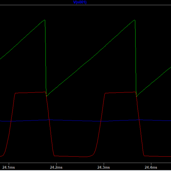
Pulsing Current Ramp
While this is what was shown, the program demands one additional variable, 5 total.
You can also manually redefine the x-axis as a parameter other than time, and similarly, redefine axes to be time
EP 5 – Stock example simulations to play with
https://youtu.be/MwfeMjcM4zY
There are plenty of example circuits provided in LTSpice
First, there are inbuilt circuits that demonstrate the operating condition of things like opamps available when selecting the component
Then, there also Educational examples and transistor level layouts of common chips, as well as standard circuit configurations
NE555 Timer Transistor Level Layout example
EP 6 – Basics of FFT analysis and the .four statement
https://youtu.be/rVAvW1Jh2AE
Setting up a basic AC signal to check Fourier Analysis on
Right click the graph zone and View > FFT
You can select multiple signals to analyze on the FFT graph
Even though this is supposed to be a pure, perfect sine wave, the simulation will show something choppy
Because this is a computer simulation that is actually sampling a pure sine wave, some parameters need to be changed so the sampling occurs with more precision. This will result in a cleaner FFT graph
First, numdgt is how many digits of precision are used in the calculation. the default is 6 so setting it to 7 will double the precision
Second, plotwinsize represents how much the data points on the graph are compressed. the default value is 300 but manually setting it to zero results in no compression.
Another issue is the maximum timestep for the graph. You can manually set the maximum timestep to something like 100ns, and that will increase the resolution of the graph, at the cost of increased computation.
Finally, the simulation’s run time is 10ms. This results in a minimum frequency of 100Hz, and so every frequency on the FFT graph will be a multiple of 100Hz. By changing the simulation run time to 100ms, increased computation occurs, but the minimum frequency is now 10Hz, which means the FFT graph will plot in increments of 10 Hz
After some tuning, here’s the improved FFT graph
The .four command can be used to perform harmonic analysis on the circuit. It requires a separate .four command line that runs alongside the .tran simulation, and then the results are stored in the error log:
Syntax: .four <frequency> [Nharmonics] [Nperiods] <data trace1> [<data trace2> …]
Example: .four 1kHz V(out)
Video Example: .four 100 10 100 V(reference)
1000Hz, 10 Harmonics, 100 Periods, V reference
The Error Log can be found under View
It’s worth noting the frequency of the harmonics, the fourier component should be 1.00000, along with the normalized component. Same with phase being 0.000. As the base sinewave, this fundamental frequency acts as the reference for the rest of the analysis. The most important number is the THD, Total Harmonic Distortion at the bottom. In this case, the sinewave is perfect, 0.000% distortion
Common Emitter Amplifier for the sine wave to check THD changes on the amplified signal
After running FFT on the output, we can see some extra harmonics present in the output signal
And the Fourier Log also reports this, but only if you add the extra signal to the .four command
Total Harmonic Distortion of 3.07%, compared to the 0.000% of the original sinewave. This number can be improved by selecting different resistor values.
EP 7 – Dependent Voltage and Current Sources
https://youtu.be/Jn8mJG3qeoo
Types of Sources:
V – Voltage
I – Current
E – Voltage Dependent Voltage
G – Voltage Dependent Current
H – Current Dependent Voltage
F – Current Dependent Current
BV – Behavioral Voltage
BI – Behavioral Current
BI and BV just take in any arbitrary algebraic expression
Note that dependent sources cannot be referenced to passive component values. They have to be referenced to an independent source’s voltage or current. Which I find strange and limiting. I believe I may be misunderstand this.
EP 8 – Turning a datasheet into a component model
https://youtu.be/0smuo8bMRn4
There are many ways to create a model for an IC. In the 555’s case, you can either build an accurate, transistor level replication of it, or you can recreate the block diagram from the datasheet using idealized components. In some cases you can also find a Spice model from the original designers, which will include the largest amount of parameters and specifications for the model. Generally speaking, the higher the complexity of the model, the more time it will take to simulate.
An interesting consideration he takes is to look at the max and min values for things like, clock pulse length, and voltage sources, and add behavioral voltage sources that have logic to disable the output if those operating ranges are exceeded. This would ensure that your model will indicate to you if you’re trying to use the IC in a way that it wasn’t designed for.
This is a grueling process
EP 9 – Independent Voltage and Current Sources
https://youtu.be/nPZ7vneN3v8
Current sources have to be connected to a load or you’ll get an error, obviously
Voltage Sources have the following Parasitic Properties
Series Resistance
Parallel Capacitance
Current Sources only have one parasitic property, and that’s to check it as an Active Load. This means it will not generate 1A of current, but will instead PULL 1A of current from whatever it is connected to.
Voltage Sources have 6 different functional modes
PULSE, for creating PWM/Square Waves/Triangle/Ramps
SINE, for creating sinewaves with offset, frequency, and decay
EXP, for creating exponential saturation curves, like RC decay
SFFM, for Frequency Modulated Signals, with Carrier and Modulation Frequencies
PWL, for Piecewise Linear, which requires a list of time and voltage coordinates to interpolate from
PWL FILE: which takes in a .txt file for PWL data, or can pass in a .WAV file from a piece of audio. This can be useful for testing amplifiers
PWL FILE can also be called on to repeat forever, or repeat for 2, etc.
EP 10 – .wave statement and Audio File Processing
https://youtu.be/mdJm-TzrBsA
The .wave statement will take whatever signal you are simulating and output it to a specified .wav file
Syntax: .wave <filename.wav> <Nbits> <SampleRate> V(out) [V(out2) …]
Example: .wave C:\output.wav 16 44.1K V(left) V(right)
One very important specification is that the circuit’s output signal has to fall within +1/-1 Volt in order for the file write to work properly
So, you can import files, and then distort or filter them, and then re-export them into a new file
EP 11 – The effects of temperature on your circuit
https://youtu.be/VzxnNrOMcMo
Capacitors and Inductors have a series resistance that changes with temperature
Resistors are also thermally influenced.
As are diodes, zener diodes, transistor thresholds, opamp thresholds, etc..
In order to make temperature measuring circuits, it may be necessary to define the temperature for an individual component to simulate it sensing some heat or cold separate from the circuit. In this case the best way is to define the parameter temp=LocalTemp for that component’s value field, and then define LocalTemp somewhere else.
EP 12 – Modeling a DC Brushed Motor
https://youtu.be/Wc4XzTrWSpo
This is the first video that I felt I was not in a position to fully understand it’s content today. Since there are 21 tutorial videos total, and the rest of them fall under progressively more niche categories, I’m going to switch gears a bit and start actually modeling in LT Spice.
4
Tutorial Sites
Asicworld
ZipCPU
Nandland
cplusplus
Practice Problems for Hardware Engineers.pdf
FPGA4Fun
Nandgame
HDLBits
EDAPlayground
FPGA4Student
Bitsolver
5
Art of Electronics
5
Automate Boring Stuff with Python
6
C++ for Embedded Systems
6
3D Printing Dive
C
Bed Adhesion Issues
Prints were coming out real good but the PEI sheet I put on the glass bed was significantly worse than the glass bed. This hot glue gun holder I printed snapped itself before it would unstick
So I took the sheet off and to remove the insane adhesive it came with, I wrapped the bed in paper towels and soaked them in everclear for about an hour, then it rubbed right off
though i’m thinking either the adhesive or the alcohol might’ve chemically damaged whatever top coat they put on the glass, since the surface scratches way easier now. I don’t really want to buy a new glass bed, but it looks like there’s pros and cons to both
the coated side of the glass bed is more worthless than the PEI, so i flipped it over and used the uncoated, straight glass side. but using the pure glass side also means nothing will stick to it and the first layer lines will just slide around if they’re ever crossed over. The solution is to just spritz some hairspray onto the bed. Now I have a minimally sticky surface whose stickiness I can control by wiping it with hairspray or IPA. The last test print I did had perfect first layer adhesion but also unstuck with a light nudge of one finger. Going to reprint the hot glue gun holder and see how it goes
The corners and edges of the print would eventually unstick and warp upwards due to the heat. Unfortunately, it looks like the PEI laminate sheet was the lesser of the evils here, so I had to order another one. I’m not sure if this was a worthwhile experiment or not.
Retuning new PEI bed
Applying a new PEI sheet. It recommends 60 or 70 C for the bed. Which may be part of the reason why I was having trouble before
This time, I’m applying the PEI sheet onto the bed separated, and onto the boro glass directly, not onto the coated side.
After that, I’m going to heat the bed to 60C and apply pressure using a textbook and a towel
Then I’m going to relevel the bed, and rerun temperature and retraction testing based on a 60/70C bed temp
Temperature testing GCode generator was glitching so I just gave it a skull to print. Generally, it looks as good as it did before, maybe a little better. Retraction seems to be worse than it was before though
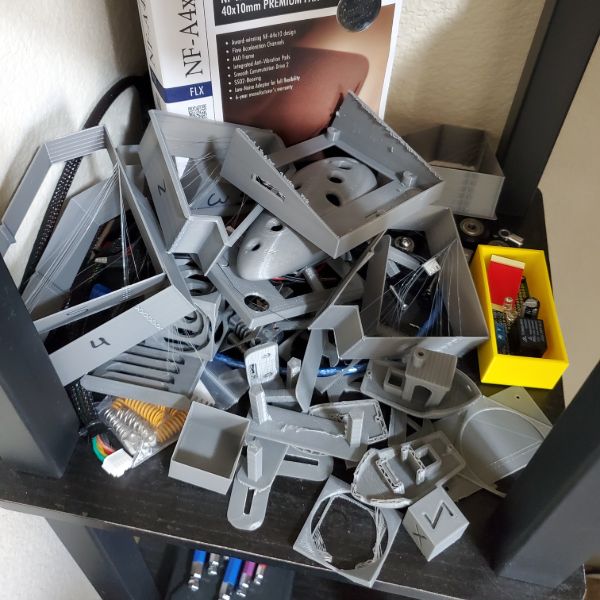
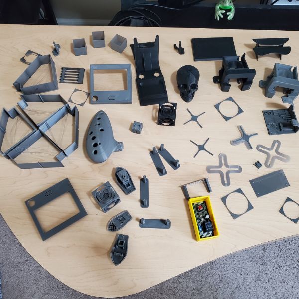
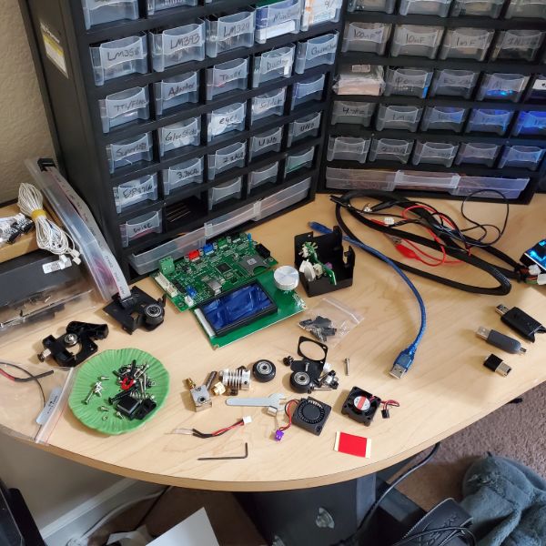
Cleanup
Threw out all the test prints and packaged up all the extra parts and screws and old pieces
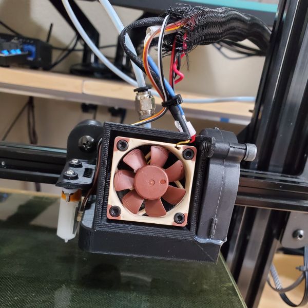
Installed the new black fan shroud and BL touch, recalibrated Z probe offset, leveled bed, and also installed black mobo.
It was a little big, so I had to melt the holes and heat the edge and then press it to squash it and deform it to a shorter length. It eventually fit with a great fiction fit though and now the mobo is rigidly mounted. Only issue now is the USB slot is inaccessible. SD slot is great though.
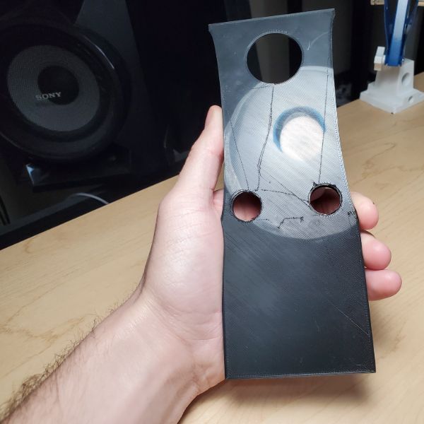
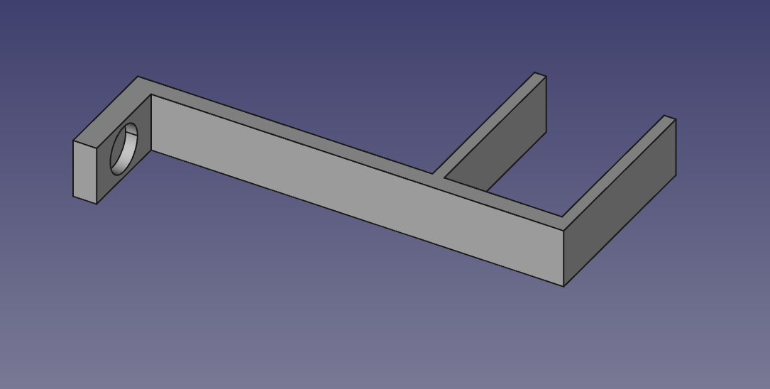
Desk Clamper
designing a desk clamper for the upper desk, that can hold something
upper desk thickness: 20mm
arm depth: 30mm
24
23.97
0.125%
74
73.68
0.432%
19
18.98
0.1%
10
9.91
33
32.8
Dimensional Accuracy
New Calibration Cube
Measurements
X
19.86-19.88
Y
19.82-19.87
Z
19.85-19.87
Deviation
Avg XYZ, 19.87
0.65%
Reprinting at 100.65% size
100.65% Dimensions
X
19.91-19.95
Y
19.96-19.98
Z
20.07-20.08
Avg XY, 19.96
Z 20.08
100.75%
100.80%
100.85%
100.80%
X
20.00!
Y
20.02
Z
20.07
Adjusted Y and Z Steps/mm
100.80% + Adjusted steps/mm
7
FreeCAD Tutorials
7
Plan for C
Power Supply Design Project
C1
LTSpice Tutorials, LTSpice Modeling Projects
C2
KiCAD Tutorials, KiCAD Modeling Projects, LTSpice Modeling Projects
D1
Power Supply Design Tutorials, Modeling along, Refining a Synth Simulation and Board Layout
D2
Power Supply Design Tutorials, Modeling along, Refining a Synth Simulation and Board Layout. Ordering PCBs and parts for Synth and Power Supply
E1
Waiting for parts and PCBs to ship. Studying more LTSpice Tutorials, KiCAD Tutorials, Power Supply Tutorials. Interview Questions.
E2
Waiting for parts and PCBs to ship. Studying more LTSpice Tutorials, KiCAD Tutorials, Power Supply Tutorials. Interview Questions.
F1
Assembling and Soldering PCBs. Designing and Printing Housings in FreeCAD. Interview Questions
F2
Assembling and Soldering PCBs. Designing and Printing Housings in FreeCAD, polishing projects, documentation. Interview Questions
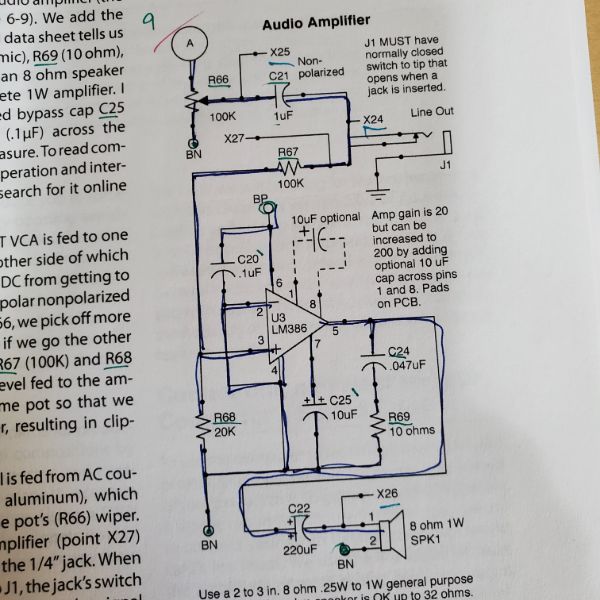
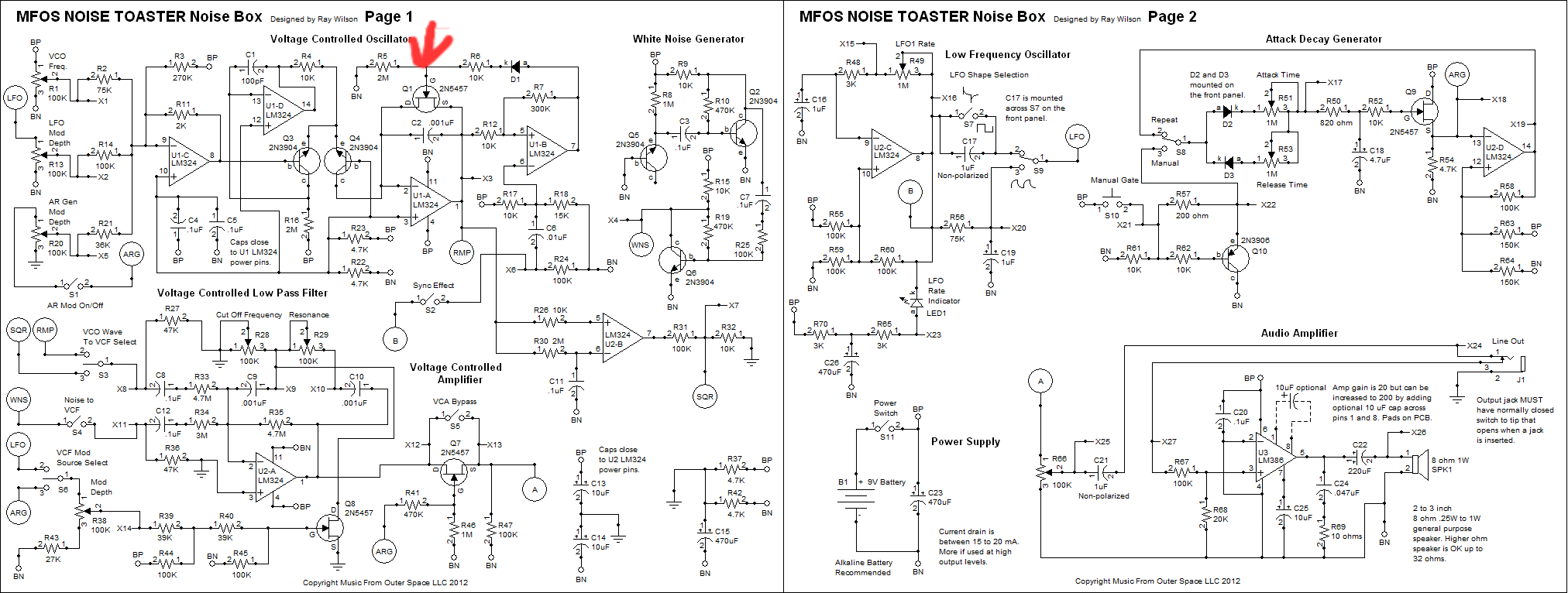
Analog Synth LTSpice Simulation
9 modules
Searching online I managed to find this website, which has a 18MB expanded library and 25MB expanded examples folder for LTSpice.
http://bordodynov.ltwiki.org/
I came across it while looking for a model for the 2N5457 JFET
That library still didn’t have a 2N5457 though, so I found this off of a forum post
https://forum.allaboutcircuits.com/threads/2n5457-spice-model.184060/
.MODEL J2N5457 NJF(Beta=1.125m Betatce=-500m Rd=1 Rs=1 Lambda=2.3m Vto=-1.372 Vtotc=-2.5m Is=181.3f Isr=1.747p N=1 Nr=2 Xti=3 Alpha=2.543u Vk=152.2 Cgd=4p M=311.4m Pb=500m Fc=500m Cgs=4.627p Kf=1.045e-002f Af=1)
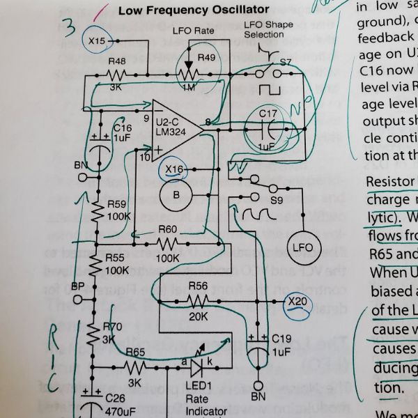
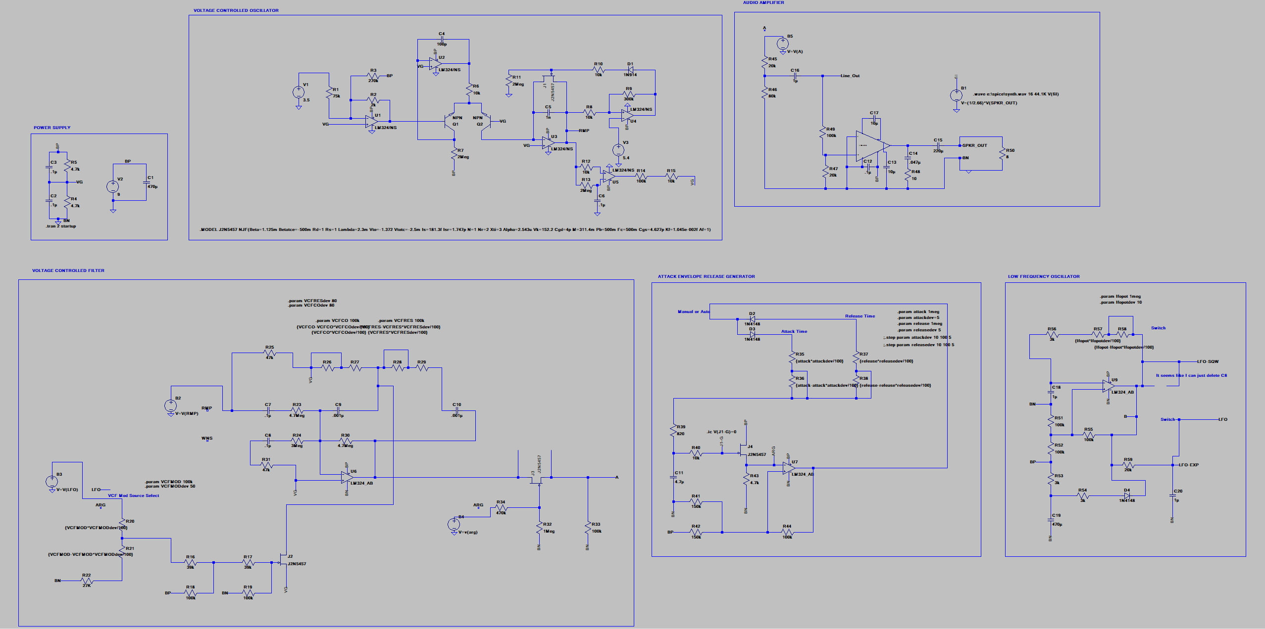
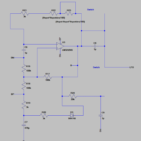
Modeled the power supply, which was easy, and the attack-release envelope generator, which was the first time I felt like I was actually doing something in LTSpice on my own. It’s nice
I’m already seeing things I was struggling to see trying to build irl and measure. For example, the virtual ground I introduced didn’t trigger the 4.5V and -4.5V split until I added a resistor network to actually create it. Also, I noticed right away that the 2N3906 was a PNP, and that it was modeled Upside down compared to the schematic.
I also was able to make good use of the .param setup for potentiometers, and the .model declaration for JFETs. All in all, the AREG worked pretty much first try.
For example, I can see the voltages and currents through every device pretty much instantly, and so I figured out the 4.7uF capacitor that’s feeding into the JFET’s gate is the thing that primarily determined the Time Constant of the AREG
This means that I could potentially pick a different cap value and then use 100k potentiometers instead if need be. The possibilities are endless and I can actually see them now.
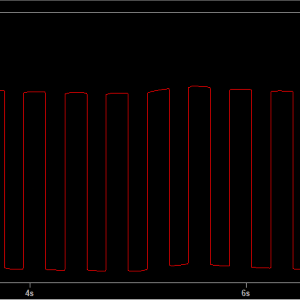
Switching the AREG circuit between manual and auto, and then adjusting the pot values is giving me a crazy amount of insight that matches up with what I was hearing before. I’m simulating the button press with a periodic, short, pulse to BP
I finally figured out why the LFO never was able to produce the differentiated graph. It can be produced not by switching the switch that claims to produce it in the design, but by taking the voltage differential between the two output channels
the diagram says differentiated output is active on the switch, but shorting the capacitor doesn’t do anything. the differential trace is found in the voltage difference between the square wave and the exponential wave
It seems like I can actually cut out the capacitor entirely C8 1uF
Having some bug issues with the 2N5457 model I’m using that says my timestep is too large to simulate it properly. It usually goes away if I just run it again. I have to model the thing for some good 15 seconds so far to make sure it’s running stable. Honestly, this is probably 10-20x faster than breadboard debugging and measuring, which I’m happy about.
I will need to find a new model for the 2n5457 in order to continue debugging this thing properly
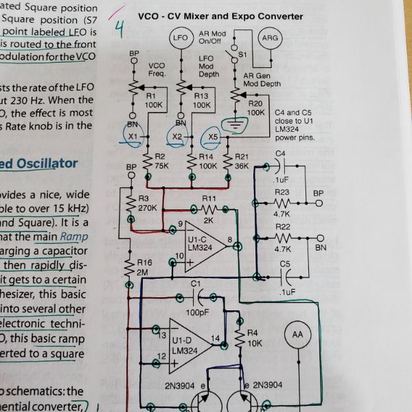
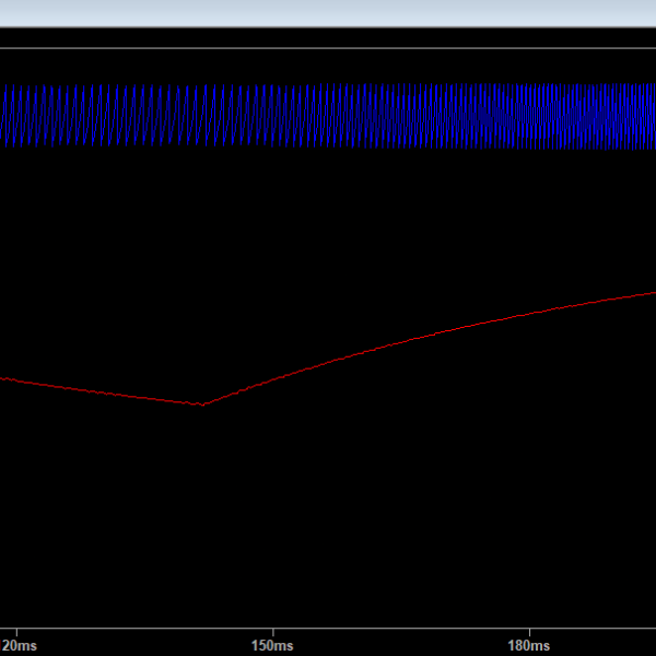
Stopping today on the 4/9 VCO Exp Mixer
I’m getting a weird jagged waveform that seems to source at the open end of AA, the audio amplifier, so I’m going to build that circuit, connect it, and see if it goes away and the VCO/Mixer fixes itself
° – ALT 0176
Breaking down the JFET Model
https://www.youspice.com/spice-modeling-of-a-jfet-from-datasheet/
JFET Available Parameters
Parameter
Description
Unit
Default Value
CurrentValue
DataSheet
AF
Flicker Noise Exponent
no unit
1.0
1
ALPHA
Ionization Coefficient
1/V
1e-006
2.543u
BETA
Transconductance Coefficient
A/V^2
0.0001
1.125m
BETATCE
BETA exponential temperature coefficient
%/°C
-0.5
500m
CGD
Zero-bias gate-drain p-n capacitance
F
1e-012
4p
CGS
Zero-bias gate-source p-n capacitance
F
1e-012
4.627p
FC
Forward-bias depletion capacitance coefficient
no unit
0.5
500m
IS
Gate p-n saturation current
A
1e-014
181.3f
ISR
Gate p-n recombination current parameter
A
0
1.747p
KF
Flicker Noise Coefficient
no unit
1e-018
1.045e-002
LAMBDA
Channel-length modulation
1/V
1e-006
2.3m
M
Gate p-n grading coefficient
no unit
0.5
311.4m
N
gate p-n emission coefficient
no unit
1
1
NR
Emission coefficient for ISR
no unit
2
2
PB
Gate p-n potential
V
1
500m
RD
Drain ohmic resistance
Ohm
1
1
RS
Source ohmic resistance
Ohm
1
1
VK
Ionization Knee Voltage
V
1
152.2
VTO
Threshold Voltage
V
-2.0
-1.372
VTOTC
VTO Temperature Coefficient
V/°C
-0.0025
2.5m
XTI
IS Tempearture Coefficient
no unit
3.0
3
I can’t seem to find my way around the instability in the circuit that causes the JFET to diverge and oscillate
http://musicfromouterspace.com/analogsynth_new/NOISETOASTER/NOISETOASTER.php#SCHEMPG1
I’ll try building it up again using the all in one schematic and referencing the webpage, but if I can’t figure it out and get stuck at the same place I’m dropping this
https://www.electronicspoint.com/forums/resources/how-to-deal-with-lt-spice-error-messages.14/
Slowly but surely figuring it out
The Singular Matrix error seems to indicate a portion of the circuit doesn’t have a pathway to ground
The circuit is based around a 9V battery being used as a +4.5/-4.5V source with a virtual ground in between
The simulator keeps having instability problems where it can’t process certain subcircuits because it thinks they have no path to ground, because they’re touching virtual ground when it expects actual ground (- terminal of the 9V) or vice versa
Thankfully, I’m starting to get the hang of adding a few components and debugging the circuit and figuring out what’s crashing the sim and why. Usually it’s fixed by adding or swapping the “grounds”
I thought it was an issue with the 2n5457 at first because it’s the component that diverges, but i don’t think so anymore.
I also thought it was an issue with the fact that LTSpice doesn’t do polarized capacitors, which led to me adding diodes to my capacitors to see if it could fix the issue, it didn’t. I think it’s the case that all Spice simulators completely ignore capacitor polarity, and I haven’t found any tutorials on how to simulate that quality either
Super critical information…
Simulation is much more stable after replacing the opamps with LM324_AB version
1:56 secrets in plain sight
adding in the Synth feels like an inflation of the project, since it’s eating up a lot of time. But at the same time, I’m getting a lot of experience debugging LTSpice and getting it to do what I want. But I am frustrated that the Synth, no matter how I try to approach it gives me a ton of issues. I’m hoping that I’ll be able to finally overcome it and get it it to work in a way that satisfied me. This thing has defeated me before and I really want to turn the tables on it. I’m learning a lot either way though. I can tell I’m getting a better intuition for circuit analysis, and how op amps and transistors work
Slowly but surely figuring it out
The circuit is based around a 9V battery being used as a +4.5/-4.5V source with a virtual ground in between
The simulator keeps having instability problems where it can’t process certain subcircuits because it thinks they have no path to ground, because they’re touching virtual ground when it expects actual ground (- terminal of the 9V) or vice versa
Thankfully, I’m starting to get the hang of adding a few components and debugging the circuit and figuring out what’s crashing the sim and why. Usually it’s fixed by adding or swapping the “grounds”
I thought it was an issue with the 2n5457 at first because it’s the component that diverges, but i don’t think so anymore.
I also thought it was an issue with the fact that LTSpice doesn’t do polarized capacitors, which led to me adding diodes to my capacitors to see if it could fix the issue, it didn’t. I think it’s the case that all Spice simulators completely ignore capacitor polarity, and I haven’t found any tutorials on how to simulate that quality either
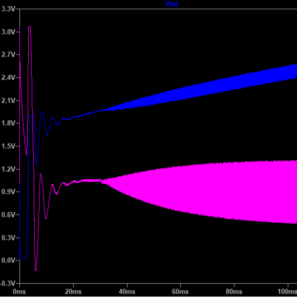
Since the circuit isn’t behaving as it should, starting around the VCO, I’m going to rebuild it using the GND node as the terminal of the battery BN, and replacing the Virtual Grounds with a tag VG
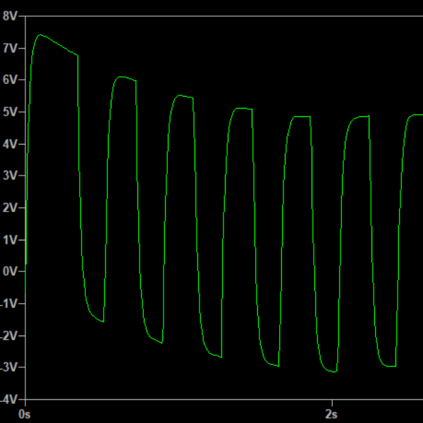
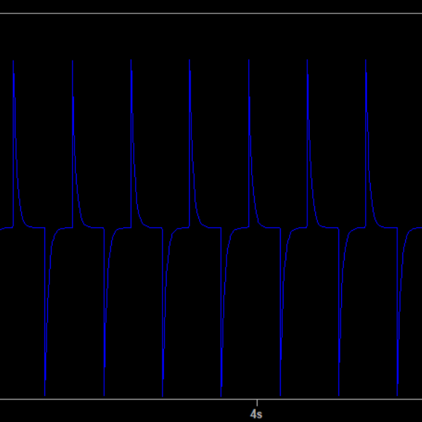
Finally got a ramp coming out of the JFET#2 with the new layout, but the simulation is still crashing frequently
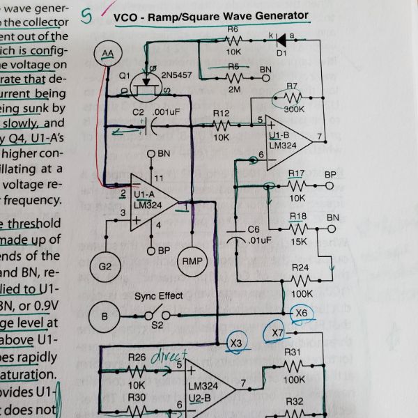
Spent a few more hours today building out the circuit again. I was able to get the RAMP function working properly. The big issue on the previous builds was that I was connecting the 2M JFET gate resistor to Virtual Ground instead of BN. When that happens, the RAMP function is unable to work properly. I made that change because without it the simulator would crash consistently. It seems like something about the RAMP function’s production is what crashes the simulator. The spike in the gate voltage that causes the JFET to short the capacitor seems to be the thing breaking the simulation.
Moving on from that, every other portion of the synth seems to simulate just fine. Since I can’t get the VCO to produce a stable, adjustable output that I expect, I can’t really test the VCF or VCA in a meaningful way. I’m not sure what I can do to get the VCO circuit to work.
I think I’ll have to go in and replace some of the components with ideal components to get it to work.
I suppose I can just get the ramp function’s general specs and then simulate a ramp output in order to move forward. but I’d really like to get the VCO working without complaint. That’s the main victory I’m working towards here.
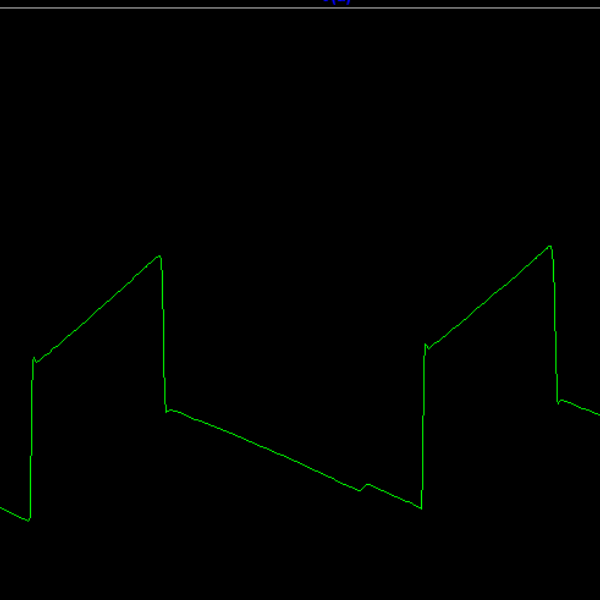
Rebuilt the VCO in isolation and it ran just fine with a generic JFET.
At 4.5V control voltage (pot at 50dev) the frequency is just about 12.5 kHZ
At 2V control voltage, frequency is 1.42kHz
after much trial and error I have figured out that the VCO is working as intended, but it has a mechanism where it exponentially converts small fluctuations into large current sinking into a cap and then switching the JFET to discharge, all to create a ramp wave. The higher the frequency of the ramp wave, the more computationally intensive the simulation becomes. The only way to continue working on the circuit in a meaningful way and verify its functional is to lower the control voltage/frequency of the VCO as much as I can
The speed of the simulation corresponds to the frequency of the ramp. Something about calculating these ramps is extremely CPU intensive and Spice hates it
Moving forward I’m going to have to keep the VCO Control voltage at a really low number for simplicity of simulation. I’ve already verified that it works at higher voltages/frequencies in isolation.
If I’m going to get the whole synth to run at once in a simulation without breaking it into submodules that’s the only way I see this working.
I’m going to have to save a copy of the VCO as its own base circuit and then build up the rest around it, and hope it doesn’t crash
Example: At 7V control voltage, VCO frequency is 41kHz, but sim speed is around 7.7ms/S, which means it would take 20 minutes just to simulate my 10S interval. Maybe the extremely slow simulation wasn’t the result of a bug, but it was functioning correctly, and it just takes that long to process..
Running the 7V for 2 seconds test gets my CPU up to 85C, 46% load, so I’m guessing that’s literally what’s been going on.
So, the system crashes even with the isolated VCO at 1V and 1.5V. 2V seems to be the lowest stable Voltage
This is with the default value JFET too. Not using the 2N5457.
After inputting the 2N5457, the sim crashes at 2V, seems to run fine at 4V. But then the sim takes longer becuase of the increased frequency
doing a visual comparison of the 2N5457 and the stock JFET’s ramp at 4V ~ 5kHz. If the waveforms are similar, I’m using the stock
2N5457
5kHz
870mV
Stock
8.5kHz
500mV
33ms/S
The difference is bigger than I was expecting. It’s good enough though
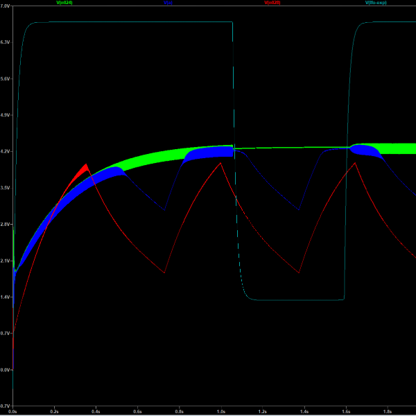
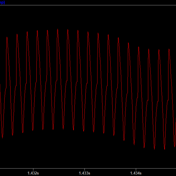
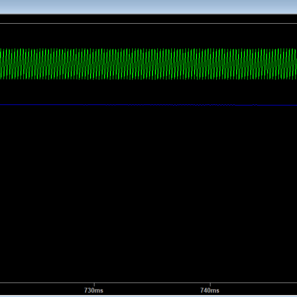
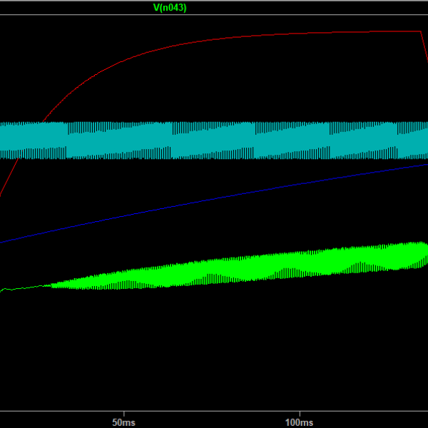
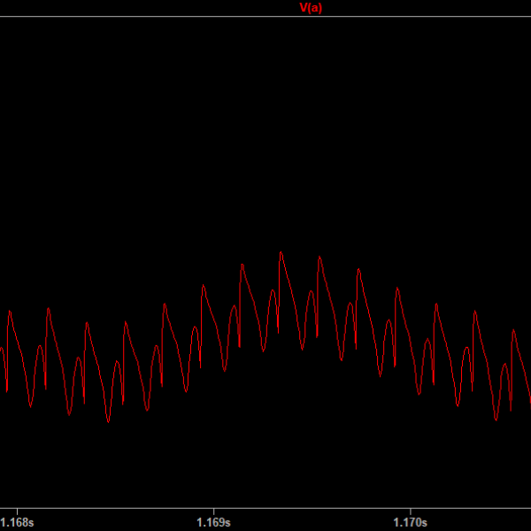
Got the SQW and RAMP wave working for a full 2S at a control voltage of 4V with the 2N5457 model. Sim speed is about 22ms/S
Added the LFO circuit and was still able to run 2S. This one doesn’t have a JFET
The B connection to the VCO does not work in the slightest. I also had to tune the set voltage for that opamp, and had to give caps an IC so they came precharged in order for the sim not to crash
After adding the AREG, which has another JFET, I’m still managing to complete the simulation, but it’s running at about 16ms/S
Next is adding the LFO and AREG to the input of the VCO, which I have a feeling will just wreck the entire thing
Adding the LFO, I was able to confirm that it works when the LFO signal is injected into the summing amplifier, but it’s unable to finish the sim. The response was as expected though. The frequency of the ramp shifted instantaneously once the LFO dropped
LFO injected into VCO input
ARG injected into VCO input
I was able to briefly simulate all three at once, but there’s no chance it’ll work consistently. I’m readjusting the VCO to be control voltage only
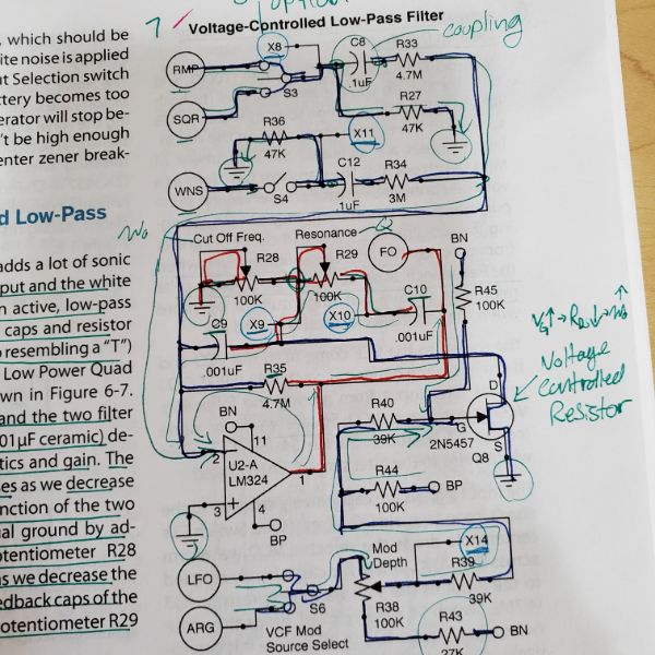
Moving onto the VCF
Verified that the VCF is working as intended using the pure ramp as an input signal.
Twisted around the pot values and achieved some different waveforms
Inserting the AREG and seeing how to plays into the filtering mechanism. The ramp input has no AREG component, but that is actually an option in the real synth so the exercise is still constructive.
Got the whole thing working
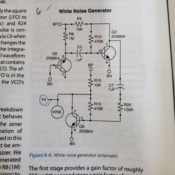
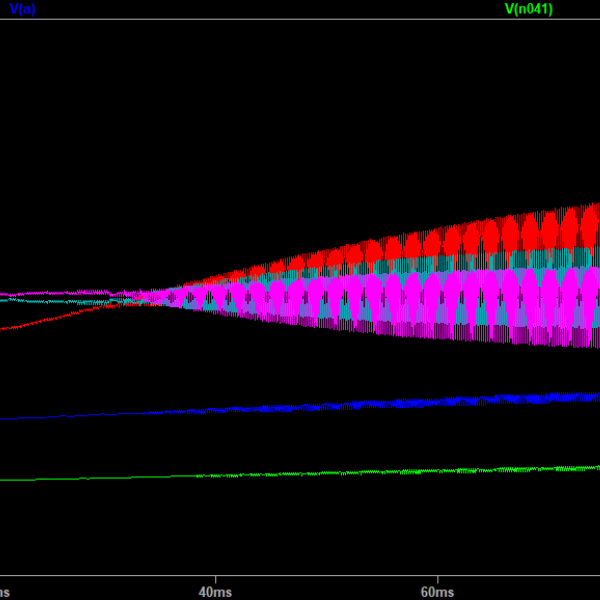
Built out the WNS. It’s strange to simulate noise, but I got it working at a level strong enough to influence the output waveform.
After that, I just dropped in the AA and it just worked. It has a singular matrix error after about 130-200ms, but its enough time for me to verify that it’s working as intended, which I’m happy about.
The last version of the synth that seems guaranteed to work is VCO-VCF – VCA – ARG working. Everything after that has a crash condition
Now that I have the whole synth functioning in one module, I’m trying to clean it up and optimize it a little.
One thing that seems to help is connecting cross-module signals via behavioral voltage sources rather than using tags. That seems to provide some isolation they need
I actually managed to complete a full 2s run with the new BV flag setup
Finally Complete!
Reorganized the schematic, added boxes and labels
Confirmed stability
Printed an export of the schematic
Cleaned up drafts and file versions organization
Added final working file to a .rar
All buttoned up and ready for presentation
I’ll have to collect all the snips I posted on discord and use those as lab pics for this sprint
Have two functional copies. One runs way faster than the other because I cut out the white noise simulator
The fastest I can get a stable version to run a simulation is about 12ms/s, which has made this whole thing pretty rough
I also only just realized my project folder is 2GB because this thing manages to produce 200MB of data after a full two second run. Something about that ramp wave generator really doesn’t get along with SPICE
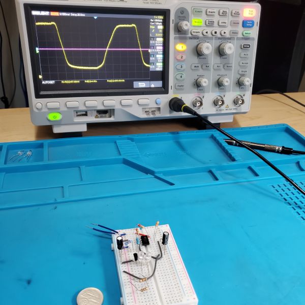
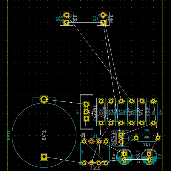
Next is to breadboard it again now that I have an effective sim to check against, and then build out the PCB
General Project Timeline
1
Watch Power Supply Design Series
2
Follow Tutorials to LTSpice
3
Follow Tutorials to KiCAD
4
Apply Tutorial Knowledge to Power Supply Design Series
5
Creating a working Simulation of the Power Supply
6
Create a presentable Schematic of the Power Supply
7
Design a PCB for the Power Supply and Place an Order at JLCPCB
8
Order Parts for the PCB
9
Design an Enclosure for the Power Supply and Print it
10
Assemble and Personalize the completed Power Supply
Next is the Power Supply Tutorials, LTSpice, and KiCAD. Since the Power Supply Project is the major action item, it makes more sense to watch those first, and then learn KiCAD and LTSpice to fit the skill learning to the project.
It’ll be important to make a point to go slow and learn these softwares just as thoroughly as I did with FreeCAD, if not moreso, since they’re the actual Electrical CAD softwares.
The PCBs and parts will almost definitely have a 2 week lead time, and I can’t order them in advance while doing the tutorials, so I’m guessing this project will end up taking about 5-6 weeks. Which means I need content to work on in the meantime.
Since I’ll have the skills to schematic and simulate circuits, I think it would be worthwhile to read Art of Electronics in the meantime. It’s kind of grindy but it’ll give me valuable knowledge to move forward with.
I also want to repair the treadmill, but in case that becomes a complicated project, I don’t want to have two large open threads at once. So I’ll hold off on that.
Strictly speaking, it would be most expedient to start going over the hardware interview questions or the FPGA trainings, but I believe a thorough read-through of Art of Electronics is an essential element to demonstrating true proof of work. I’m guessing that after the Power Supply is finished, I could spend another month powering through Art of Electronics as hard as I am capable of, and probably get well through half the book. That would put me around end of March.
Around that point, it would also be constructive to start splitting my time between Art of Electronics and Software oriented work.
It feels like I’m really delaying FPGA, so that’s probably not the best plan
After mapping everything out, it looks like covering the complete list of Monty Choy interview questions will be more effective at covering an incredibly broad basis of knowledge than reading AoE with my given timescale.
With that in mind, and the limited time I have, I think it would be most worthwhile to allocate ample time to go through that list and prepare my answers for it, and then move on to FPGA specific things until the time is up. So the flow would be 3DP>PSU>Interview Questions>FPGA
One thing that I think is missing from this, is in between interview questions and FPGA I should probably have a dive into Digital Logic, Sequential and Synchronous logic elements, CPU architecture, nandgame, etc. Which would give more context to the FPGA workflow itself. I’m not sure how much of that would get covered by the interview questions and by the Intel FPGA training playlist, but I am concerned there will not be a complete overlap between those two bodies of info
ZipCPU is absolutely packed with valuable insight and wisdom about the FPGA design process, and the pitfalls that amateurs fall into, and the differences between the mindsets that amateurs and experts provide.
cplusplus seems like a really effective reference tome
nandgame seems better and better the more I look at it
asic-world is definitely the go to for getting started
Done watching Fesz LTSpice tutorials for now. Ready to put in some actionable work. Going to model out my Analog Synthesizer following the book and verify that the modules work how they should. Ideally, I should be able to produce a synthetic noise using the output .wave function.
Since I have 3 sprints, 6 weeks dedicated to the power supply design series, I’m guessing the project breakdown will look something like this
ratio’d by youngboy NBA – https://www.youtube.com/watch?v=7ZIIWUfzm2A