
C: 1/30/2023 – 2/12/2023
D: 2/13/2023 – 2/26/2023
Summary: Big post! Very busy four weeks! Was pretty swamped around end of C, so just decided to merge C and D into one post capturing ~February.
VERY LONG PHOTO GALLERY & VERY LONG RAW NOTES BELOW
Major points:
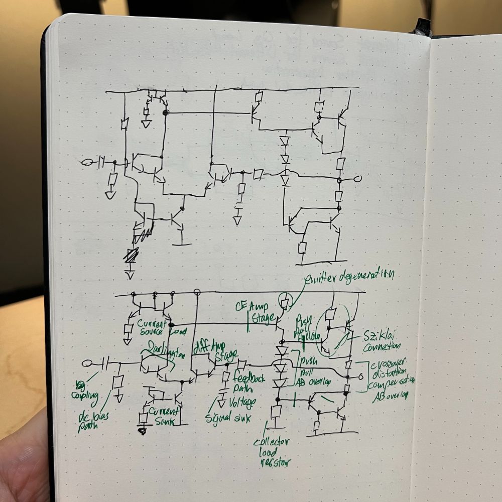
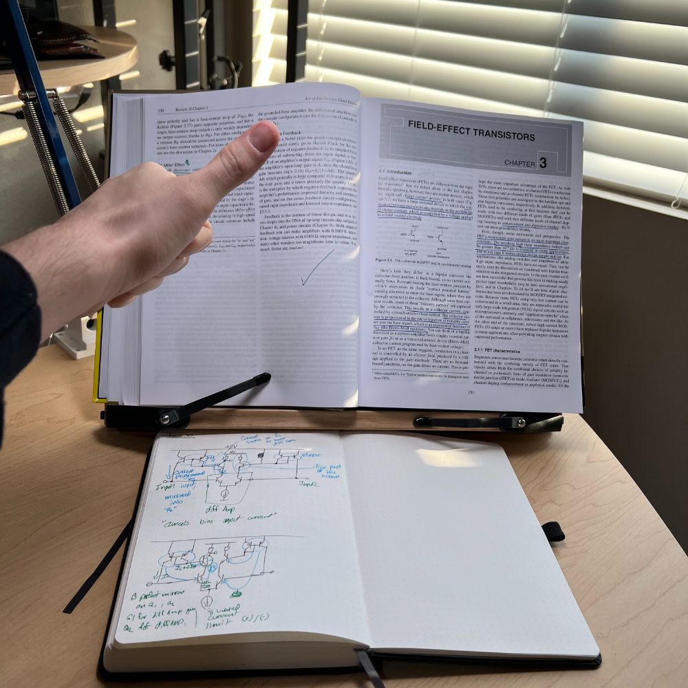
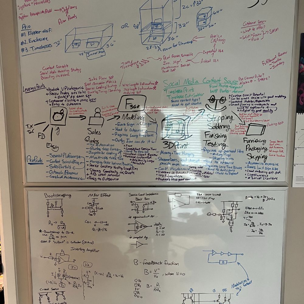
– Finished Annotating Chapter 2 of Art of Electronics (BJTs)
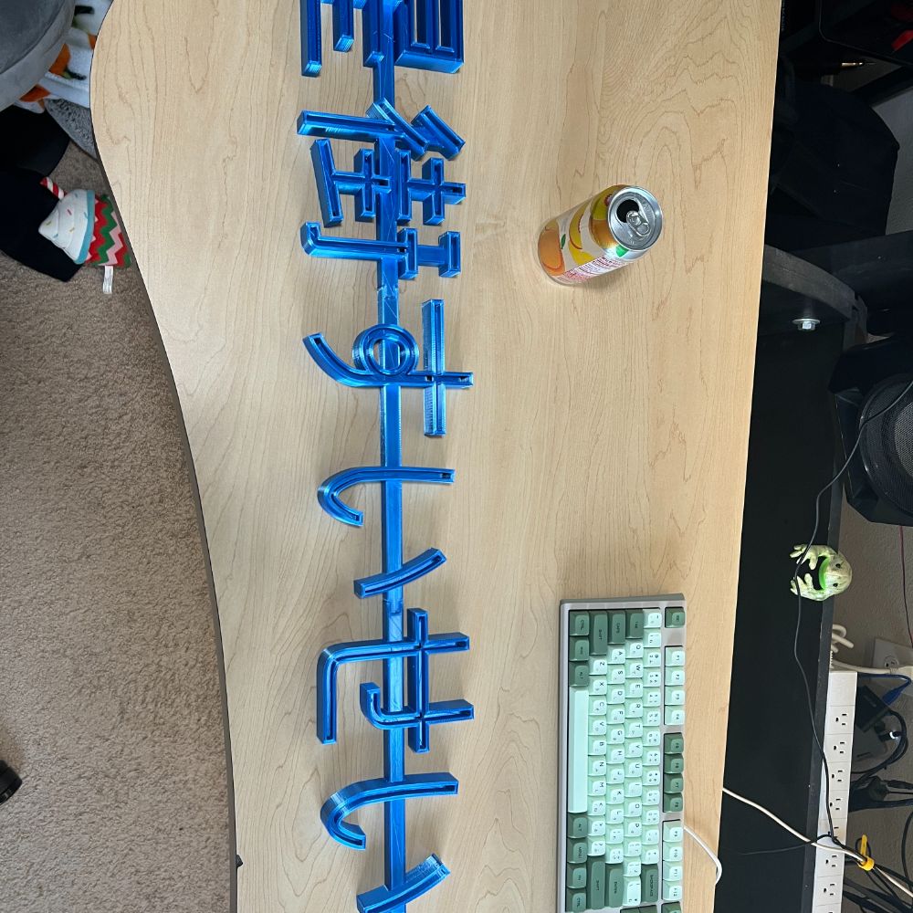
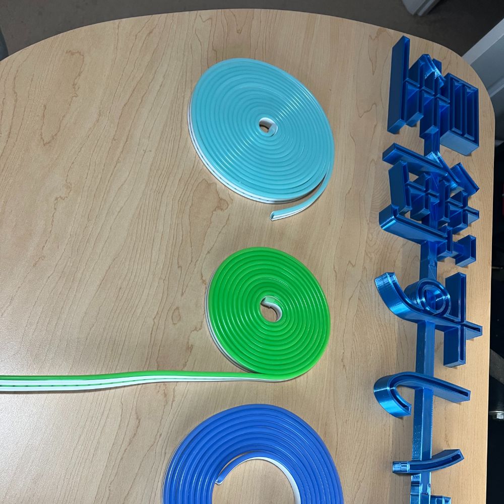
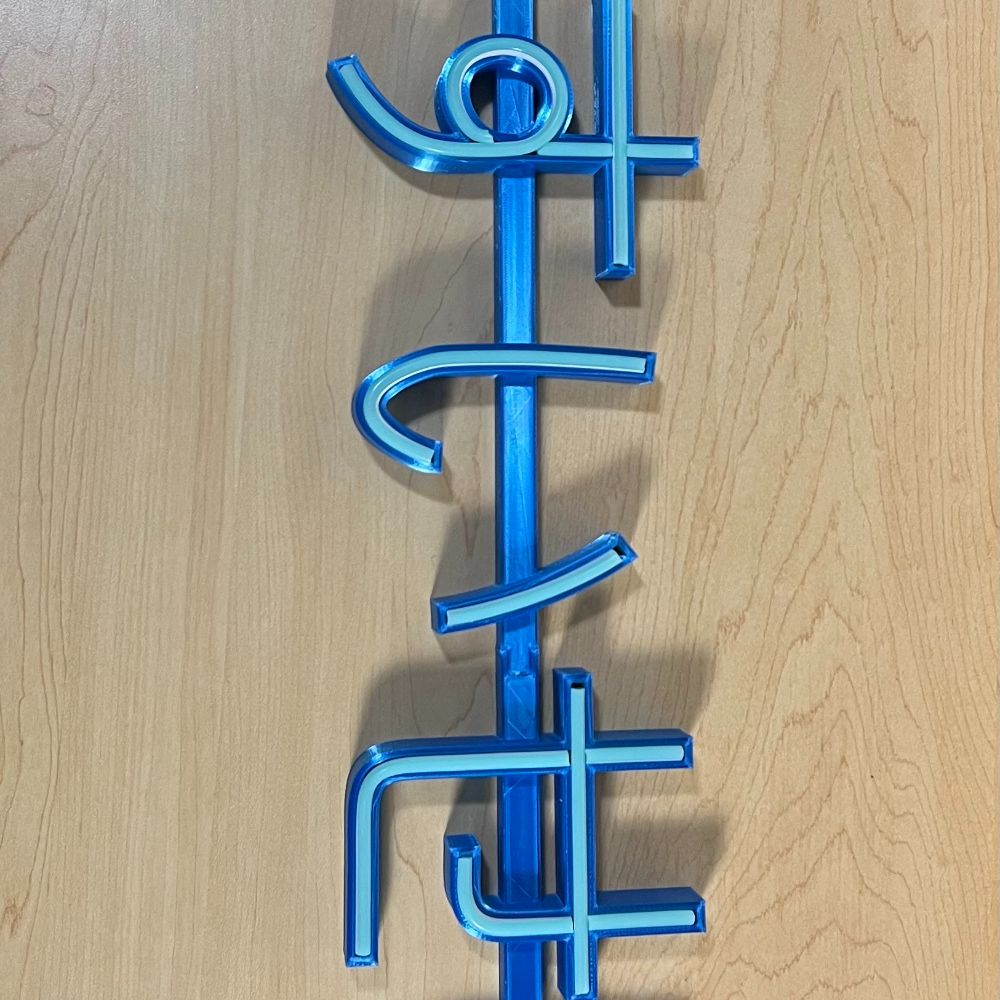
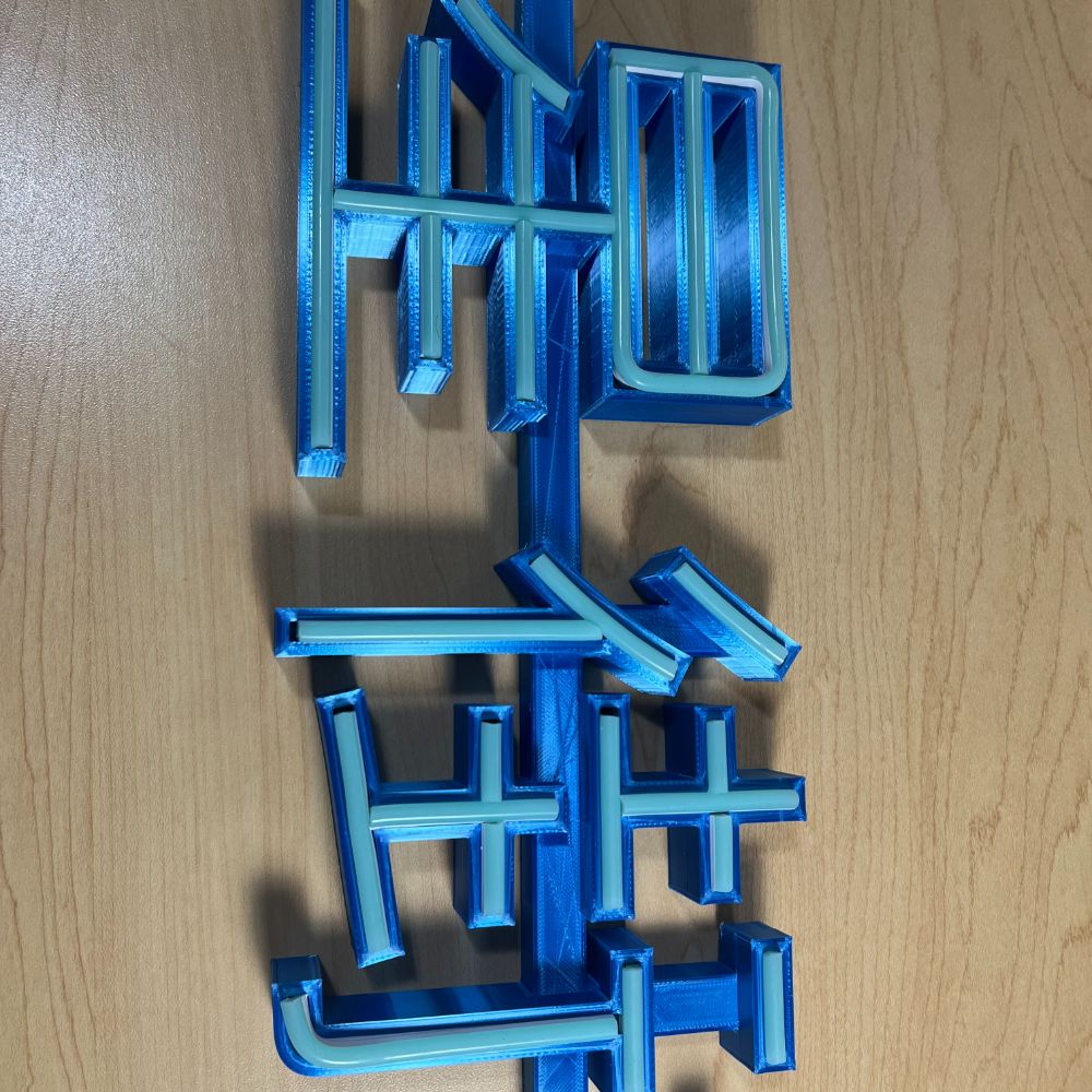
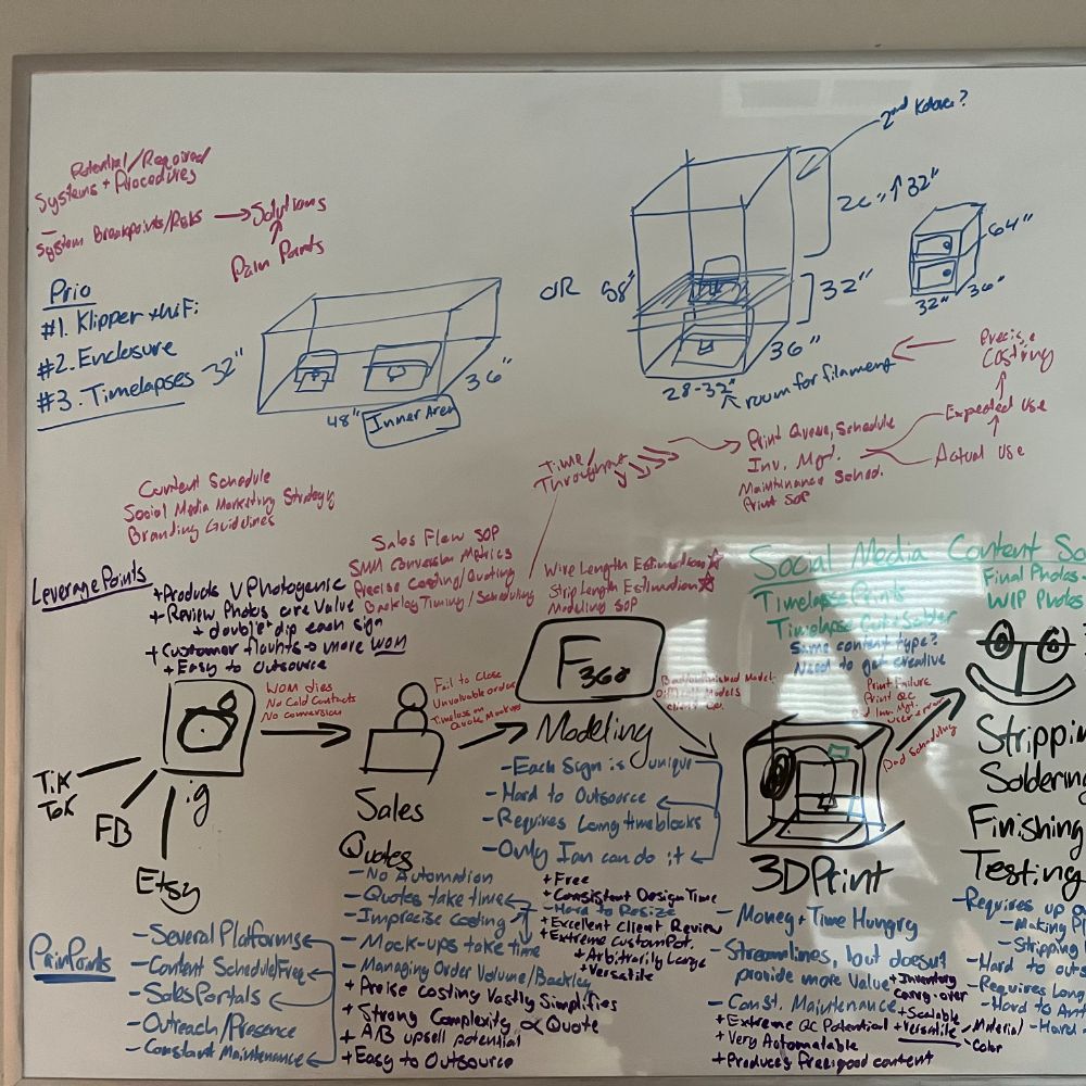
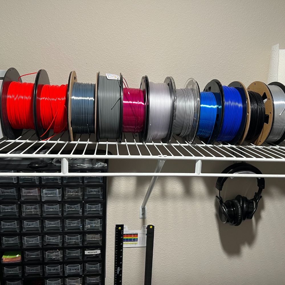
– Built out NVS SIGNIFICANTLY. Many new orders & processes + store page
– Started first read through of Chapter 3 (FETS)
– Briefly took a break to study Japanese for the trip
– Got sick
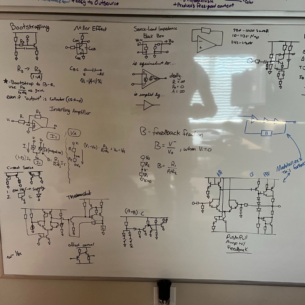
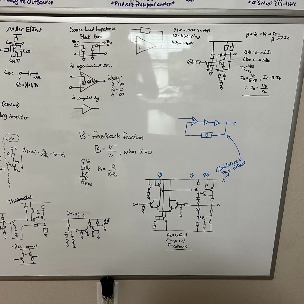
AoE Chapter 2:
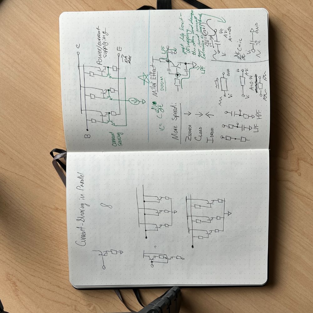
Did a great job staying consistent, woke up 5am every morning for 3/4 weeks of CD to study AoE 3 hours. Learned a lot. Made a ton of progress. Filled out basically half my notebook, finished it, bought a new one, and started filling that one out. I finished the second read through for annotation, where I figure out exactly how I would verbally explain the concepts to someone else and walk them through the logic of it, as I would in a PASS/Study Session. I am confident I can teach every detail of the chapter to someone unfamiliar. There’s like 3 concepts here and there that even I still don’t get and they’re flagged in red in my textbook. It feels good to finally make it past that. It also really started to click for me, which is awesome. I feel a lot more confident about this material now, and more confident for the book overall.
AoE Chapter 3:
FETs are a little different, the chapter is longer, in more depth, and covers way more ground. I think it’ll take me longer but will be a little easier than Chapter 2. I spent a lot of time hitting my head against a brick wall trying to get a better understanding of some core concepts in order to get through Ch2. At this point it’s just a matter of being consistent and continuing to put in the hours. I’m nervous for chapter 5 still though.
NVS:
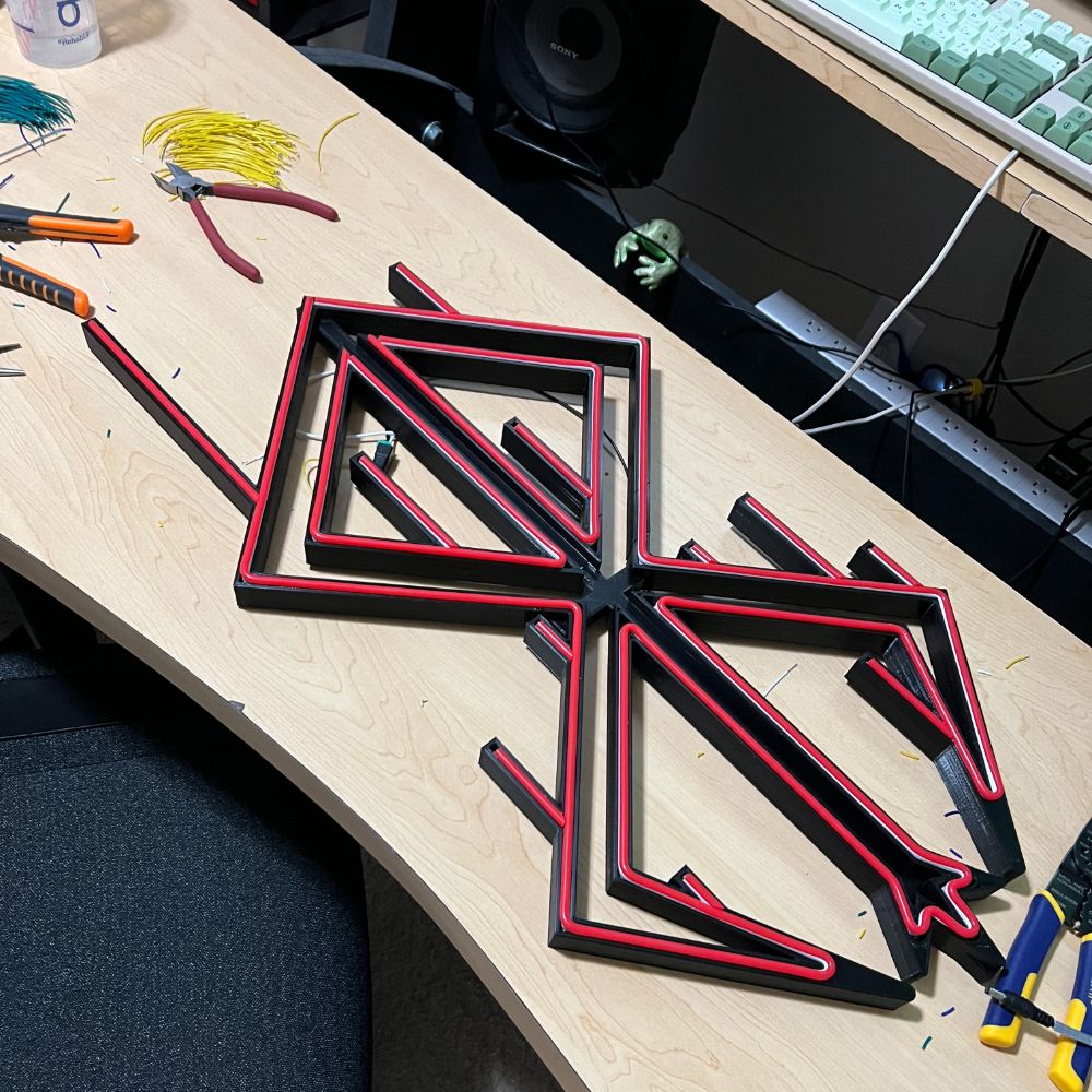
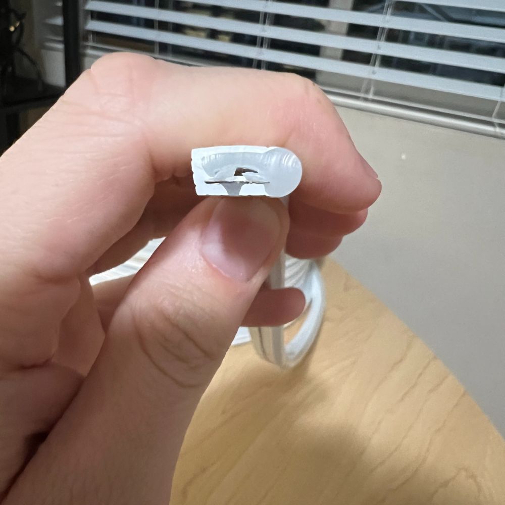
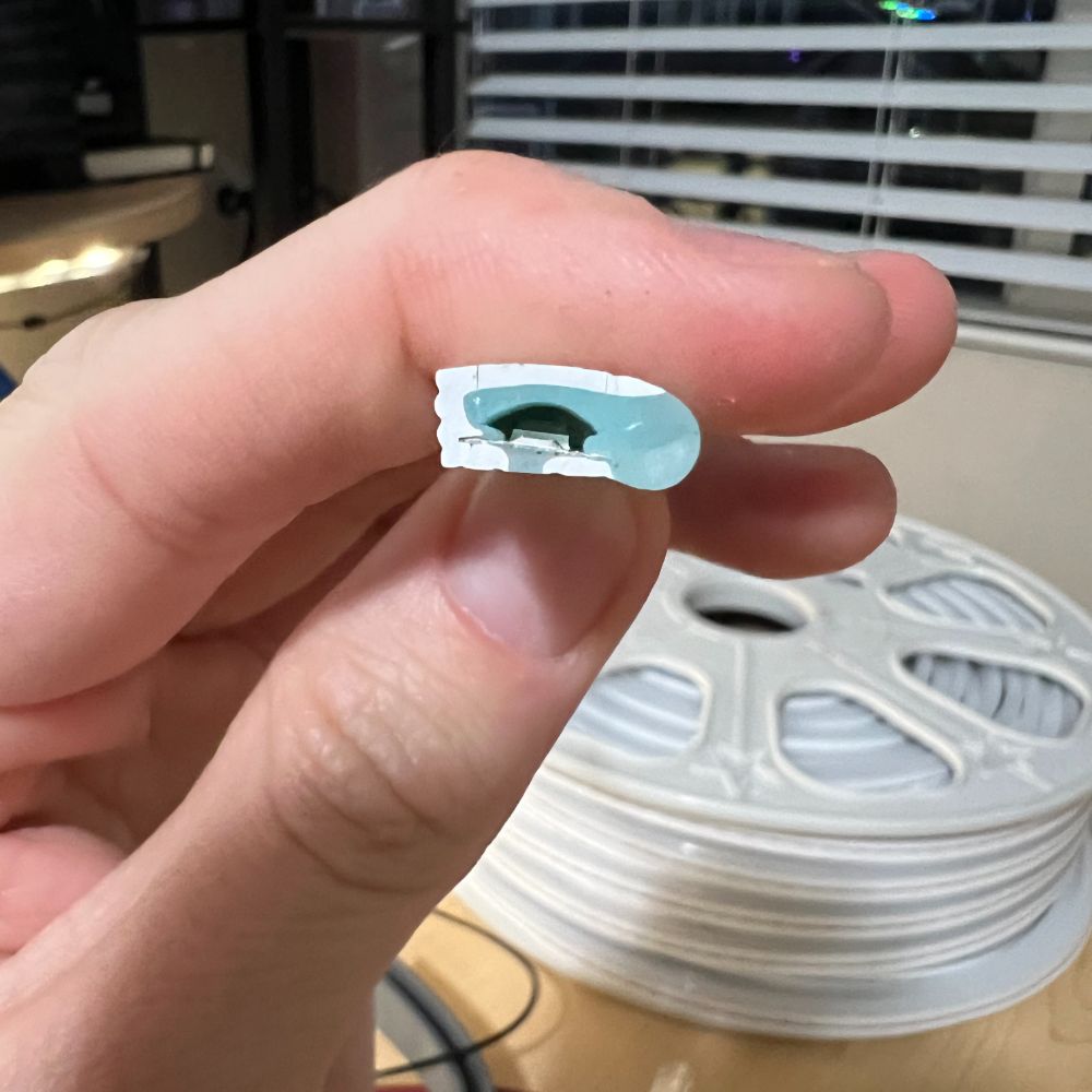
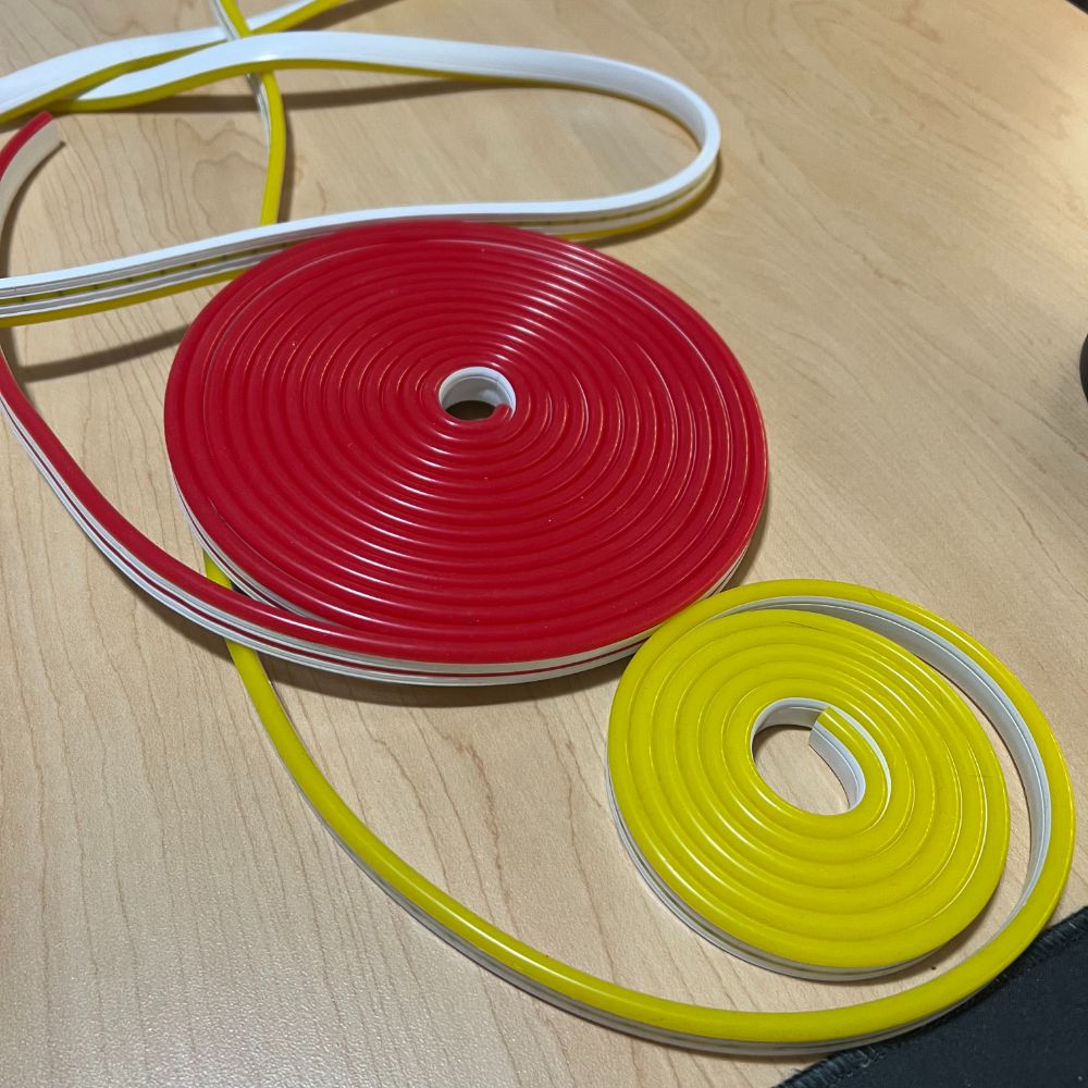
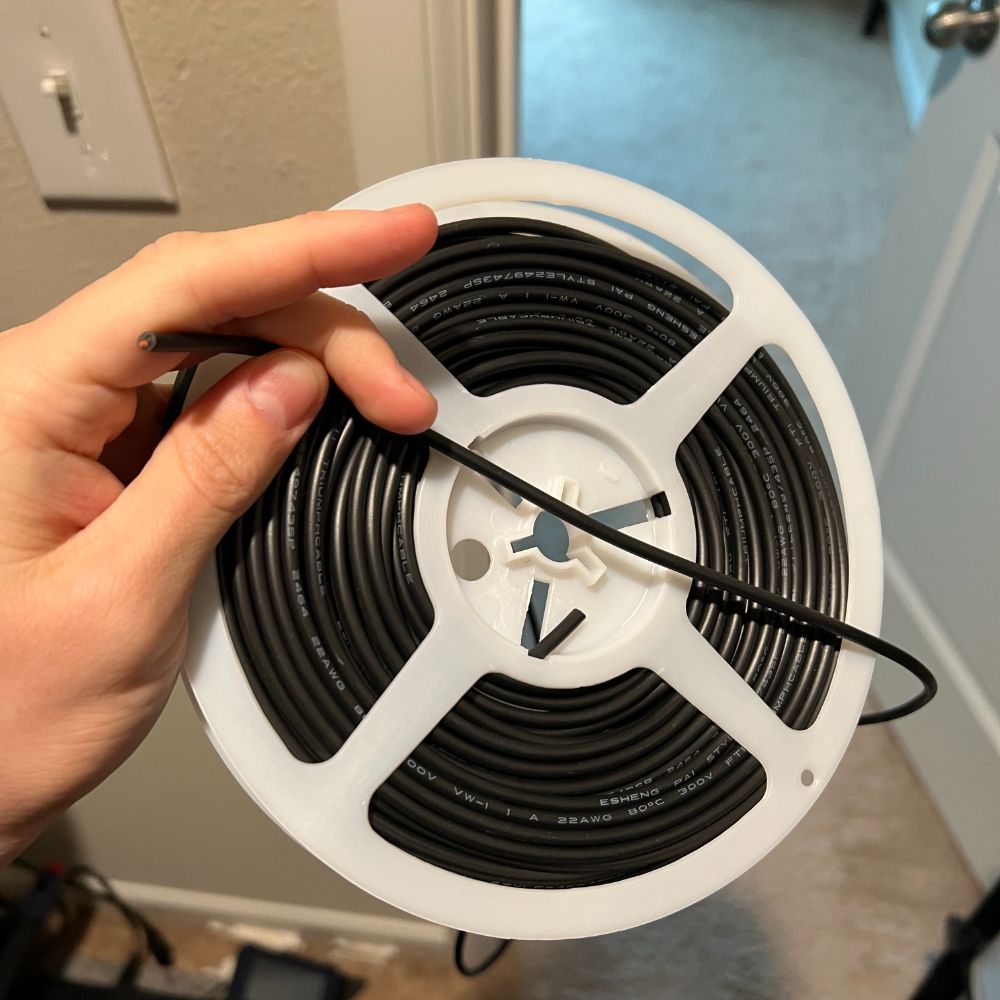
Started C with a basic master tracking spreadsheet, 50 boxes from ULine, and some money in the bank. Since then I’ve committed about 10-12 new orders, brought in a lot more cash, and then spent some of that on upgrades to streamline things more. I made a big mistake and bought a 50m roll of 6mm white strips, not realizing I’ve been using 5mm strips this whole time. To be fair though, most 6mm strips actually measure in around 5.5mm. My primary supplier on Amazon is still selling all their colors except for cool white, which I obviously need more than anything, so it’s been pretty frustrating. I’ve ordered and received two 5m samples from different suppliers at the right 5x12mm dimension and have a path forward. But it made me feel dumb lol.
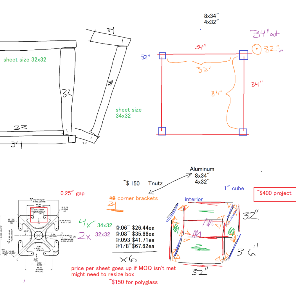
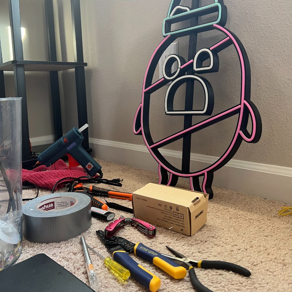
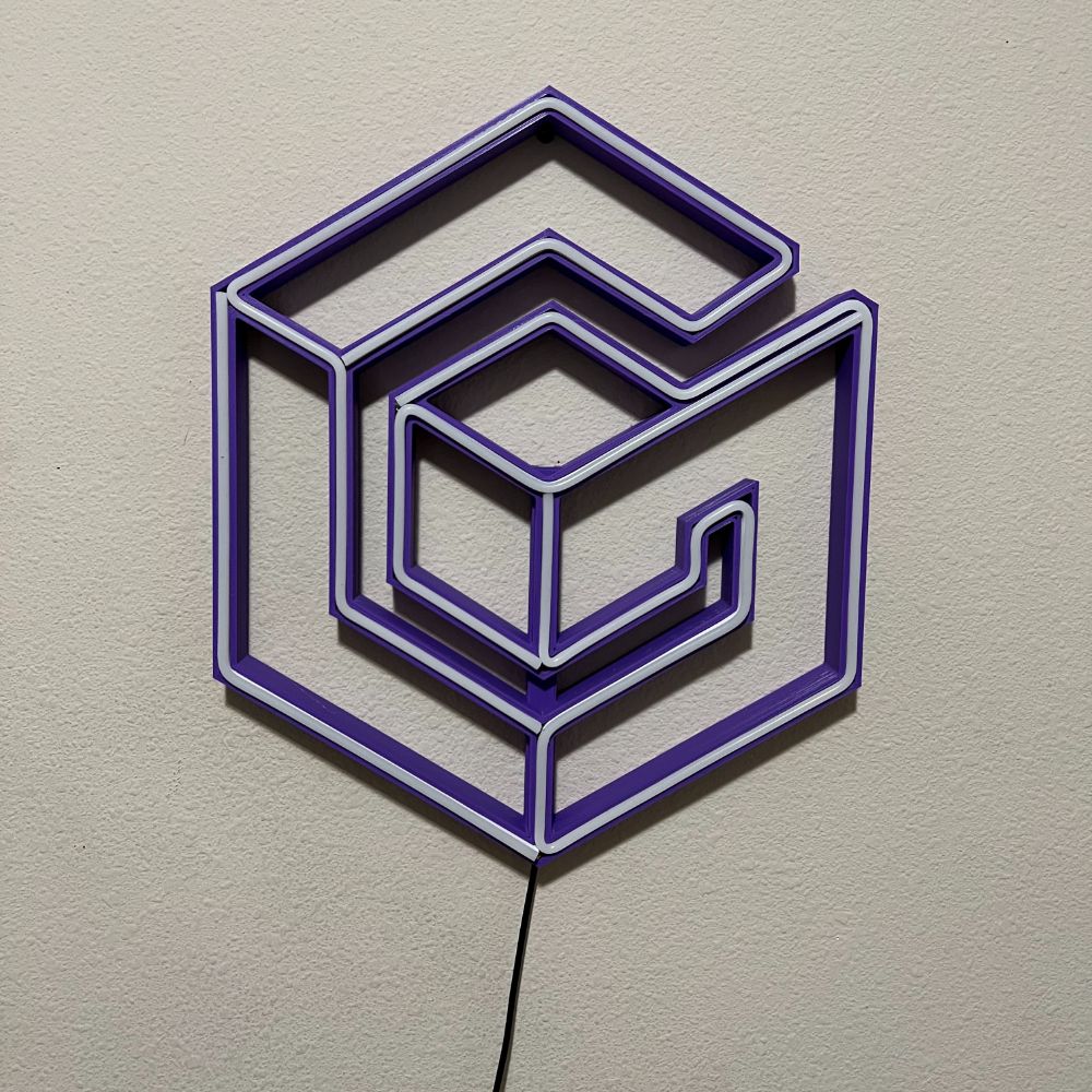
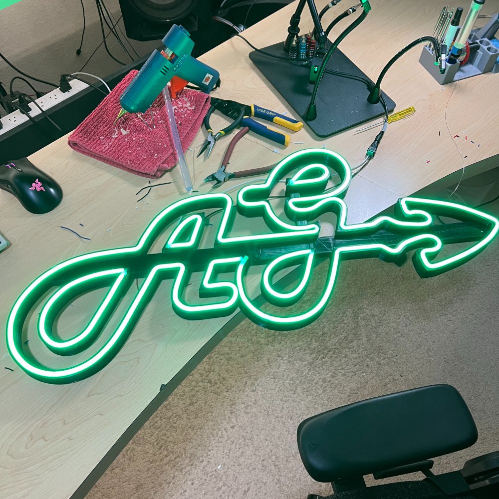
On the bright side, my BJJ gym owner told me he was interested in getting a large, 12×4′ sign done, and installing it outside on the front of the building. That would be a great use for the majority of the 50m of otherwise useless lights I have (I could redesign the channels for them too, if I needed to, but then I’d have to keep track of my 5.5mm vs 6mm channel designs and that’s a nightmare). It would be a huge order, but it sent me down a huge R&D rabbithole trying to figure out exactly which filaments I can use to handle extremely long term exposure to the Washington elements: beating sun around 90-100 degrees + sunlight + UV + strong winds + extreme rain + snow + freezing. I think PETG is the move, but I’m not sure if I can like, impregnate it with a resin to make it tougher or something. There’s also the issue of handling all the ampacity and wiring for the back, and also the issue of mounting a printed piece of hardware to the outside of a building in a secure way that can reliably remain there for years. It seems pretty narrow, but I’m confident it’s possible. If/when I pull it off it’s going to be a level up for the business and open a big door for outdoor stuff like that.
We’ve rebuilt the master tracking sheet another one or two times with new metrics as we figure out what’s important and worth tracking, and convenient, etc. I’ve also come up with a couple different ways of accurately estimating the variable material costs that go into a sign before we commit to it, to help make quoting and estimating our costs overall easier. And another system to figure out the actual materials used after the sign is done. It’s ultimately pretty simple, but there were a lot of questions for what’s going to be the most convenient, simple, and accurate method. I got pretty creative with some dimensional analysis.
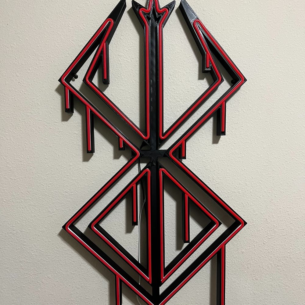
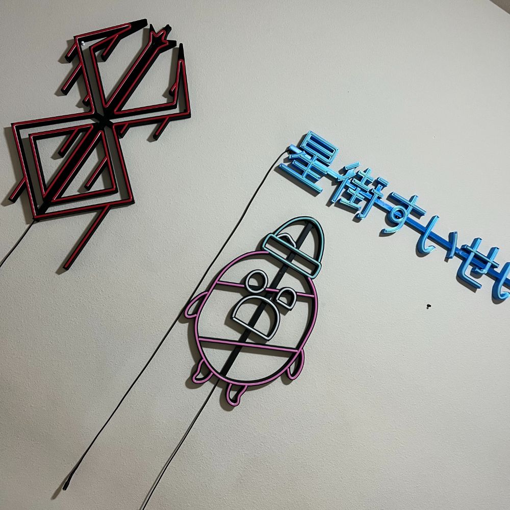
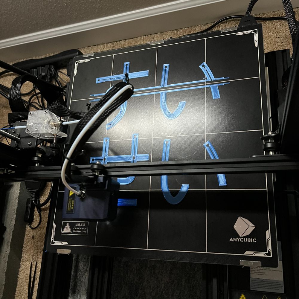
One of the signs I did went small-viral in Japanese twitter circles, and now Angel and I have been figuring out how to ship things internationally, and if it’s worthwhile. We think we have an answer: sure, but it’s gonna be prohibitively expensive. Which kinda sucks. I’d love to deliver for more people.
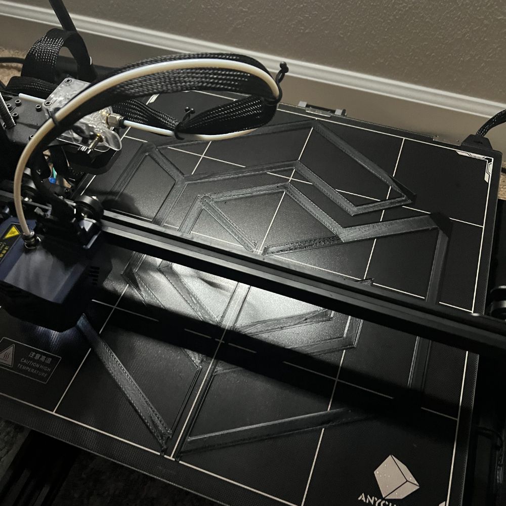
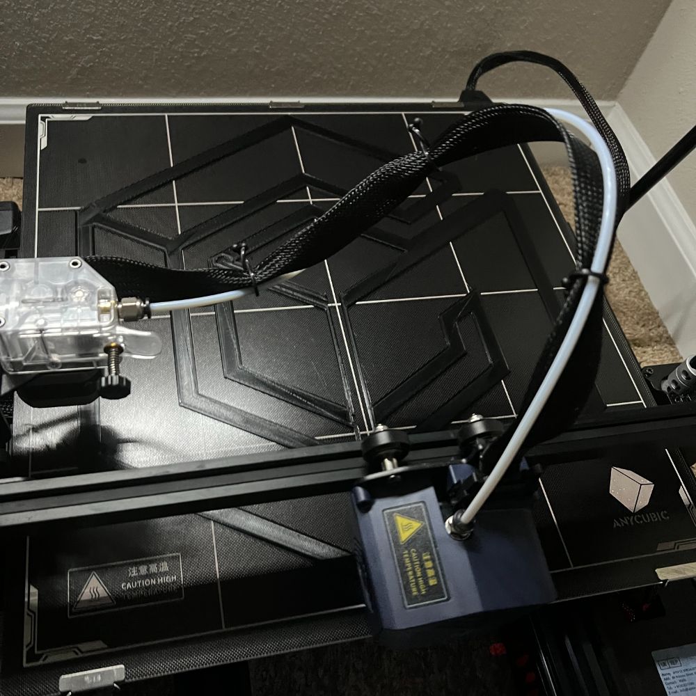
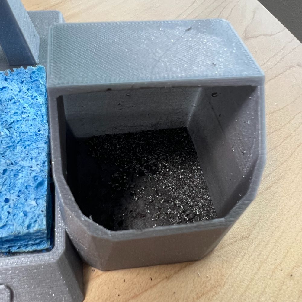
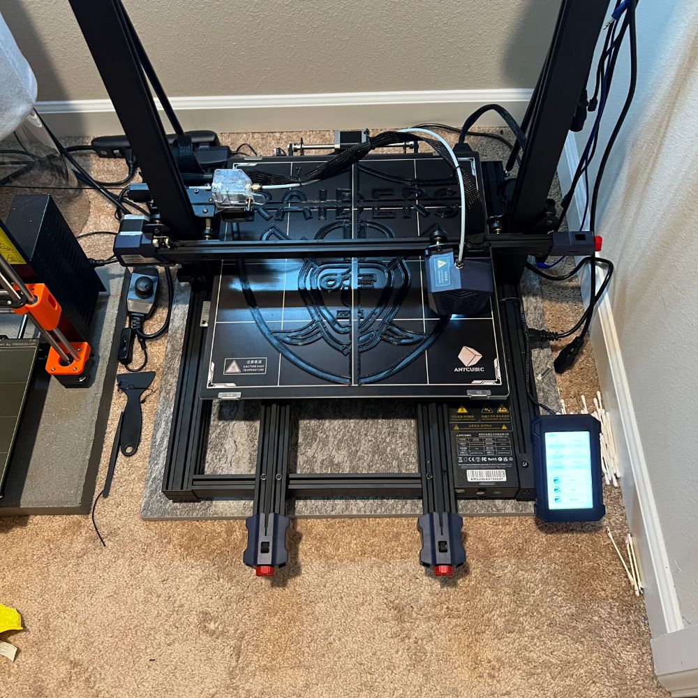
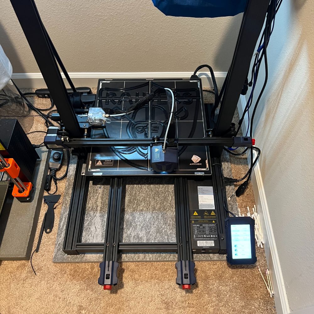
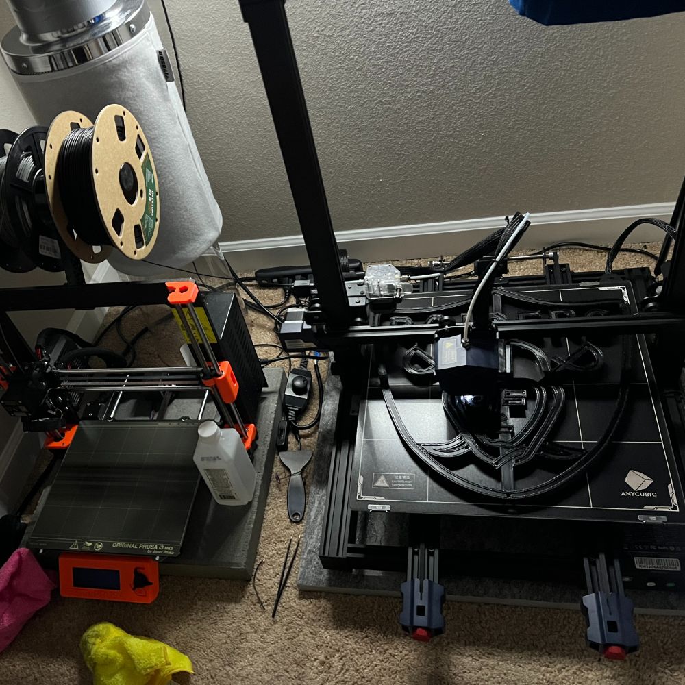
I also did some research on Klipper firmware and the Bigtreetech Manta boards. And ultimately decided to reinvest some of the funds into buying the M8P. It should increase the quality of the prints and 2-3x the print speed. I haven’t meaningfully calibrated the printer yet, I really just took it out of the box and got to work. There’s been some inefficient maintenance I’ve had to take care of with the printer because of that, and because there’s a giant ventilation fan blowing right next to it. Sure, it takes the PLA microplastics out of the closet and stops hotboxing me with cancer flakes but that airflow dusts up the printer extremely fast. I’ve also been having issues where the heat builds up in the closet, and creates a good warm environment for very large prints like this to cool off evenly without warping. But it also means I have to be nervous about opening my closet door.
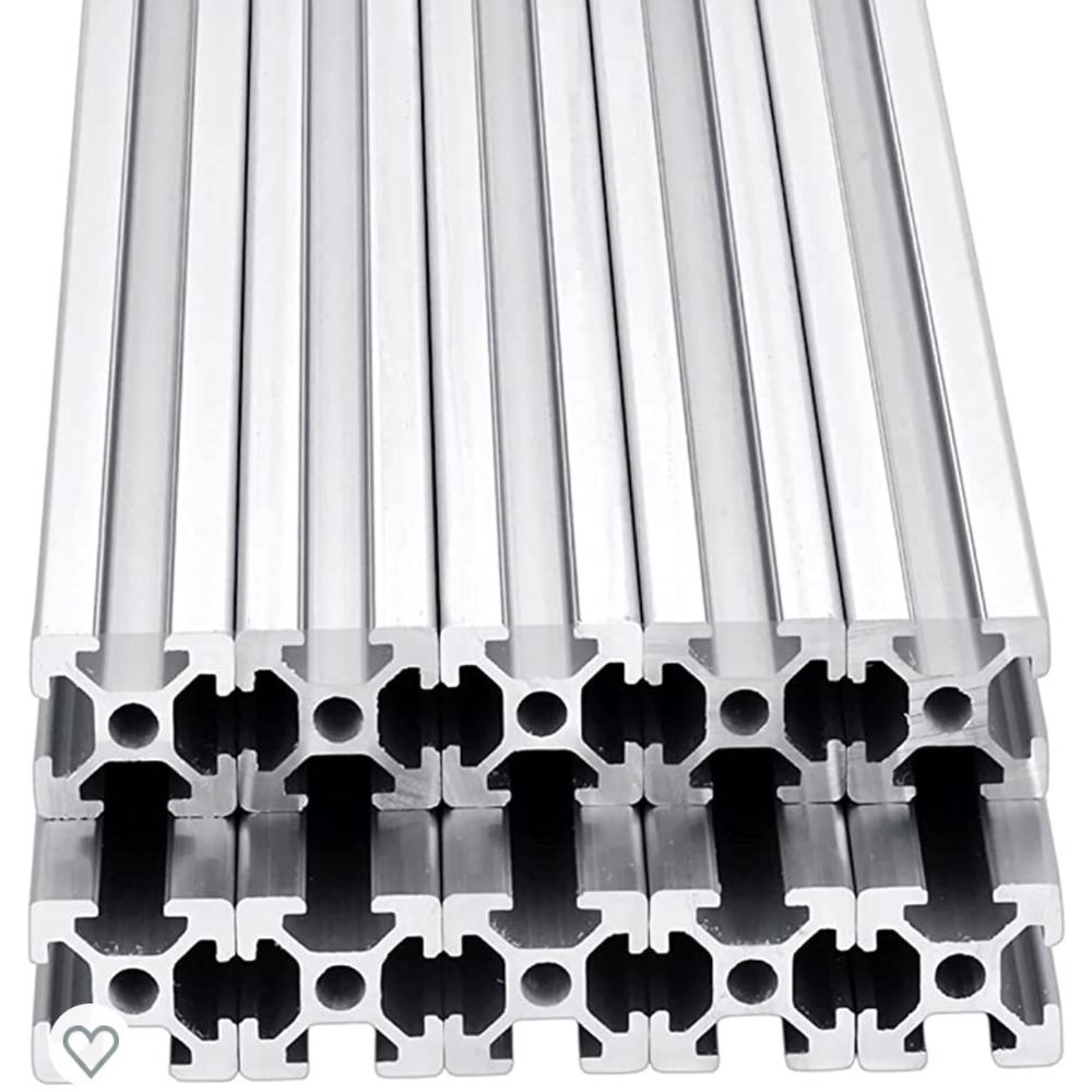
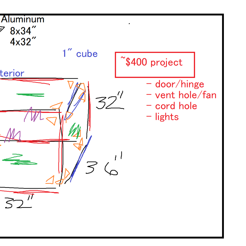
The solution I settled on is a win-win, I designed an enclosure using some aluminum extrusions custom for the printer based on a design I saw on a store that sells enclosures that aren’t big enough for my printer. It’s a win win because I’ve been wanting to find a project that lets me work with the aluminum 8020 system for a long time now and I finally get to play with it. I spent a lot of time learning how they work and the various adapters and methods that go into it. I got a lot of help from my more experienced friend Loren with sizing, part sourcing, and generally making sure my design is mechanically sound. Both the new board and the enclosure materials will be showing up during E and I look forward to dramatically upgrading this printer, and the sign quality and throughput by extension.
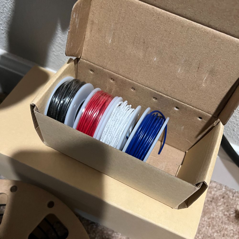
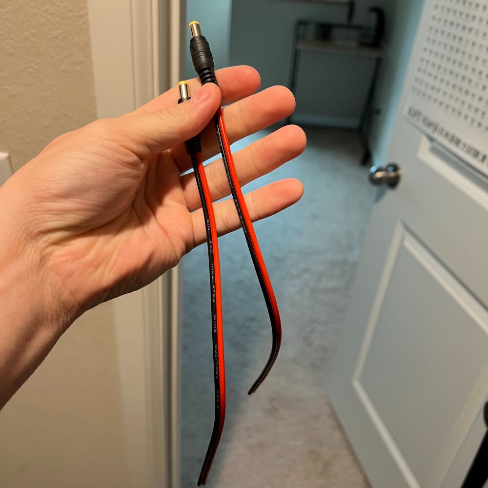
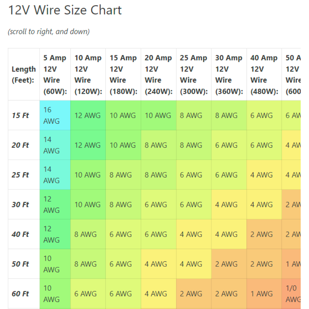
The last thing that’s really holding me up in the signs is having to manually strip lengths of wire to solder on to the strips, and making the barrel jack power cables by hand. But I have quotes for both of those on Alibaba ready to go as well. I just need a little more cash on hand to justify it. In another month or two (after Japan) this stuff is going to get much, much more streamlined. So, hoping I’m able to produce the order volume necessary to keep all this up.
Lots of fish getting fried at once these days. It’s busy, and I’m happy to have a lot of interesting things to work on and think about.


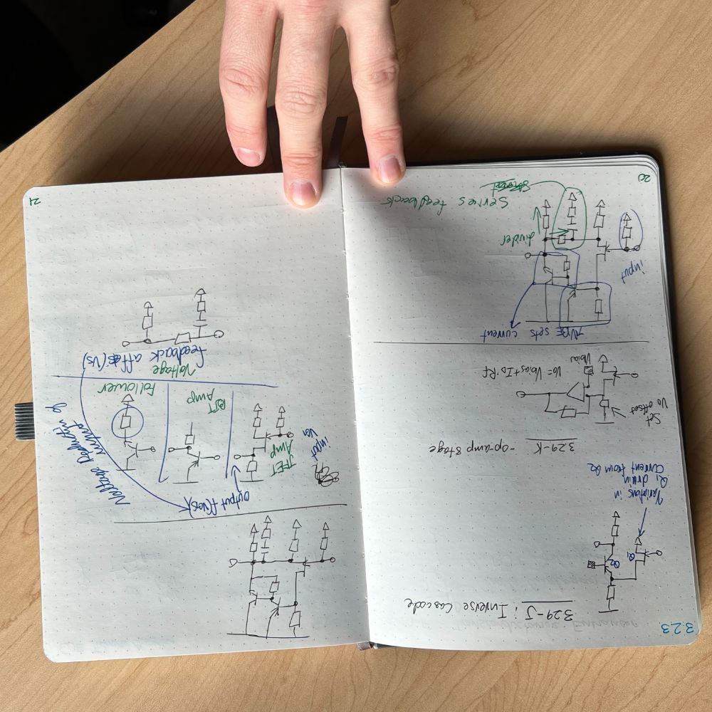


C
AOE-C
Chapter 2
2.1 – Introduction
Notes
A transistor is an active component
Active components amplify
Defined as: the output signal has more power than the input signal
The transistor is the single most powerful resource for interfacing everything in electronics – ICs, circuits, subcircuit modules, etc.
BJTs came first, before FETs in 1947
Simple comparison:
BJTs
Low noise, accuracy
FETs
Low power, high impedance, high-current switching
Transistors have 3 terminals, EBC
Emitter, Base, Collector
Vc – Voltage from collector to ground
Vce – Voltage from collector to emitter
Vcc – refers to positive power supply voltage, usually on collector side
Vee – negative power supply voltage, usually on emitter side
Vcc and Vee probably won’t change polarities if you start working with PNPs though
Transistors are 3 terminal devices, which means there are two voltages and two currents to juggle
Not 3 currents and voltages, because only 2 are independent. the third one is dependent on the other two
2.1.1 – First transistor model: current amplifier
BJTs have three terminals
a small current into the base controls a large current through the collector-emitter
comes in npn and pnp variants
NPN Rules (reverse for PNP)
1 – Polarity
Vc must be greater than Ve
2 – Junctions
Base->Emitter and Base->Collector act like diodes
Base->Emitter diode is usually conducting
meaning base is higher than emitter by at least one diode drop
Base->Collector diode is usually reverse biased
current can’t flow into the base from either E or C
Control current flows into B and out through E
3 – Maximum Ratings
All transistors have max values for
Ic – current flowing through collector-emitter
Ib – current flowing into base
Vce – voltage across collector-emitter
exceed them and it breaks
Other limits worth noting
Max power – Ic * Vce
Max Vbe
4 – Current Amplifier
If 1-3 are followed
Ic is proportional to Ib
Ic = B*Ib
B is Beta which is h_fe
“h parameter transistor model” is no longer popular
PNP Rules
1 – Polarity
Ve must be greater than Vc
2 – Junctions
Emitter->Base is diode
Collector-> Base is diode
Control current flows into E and out through B
3 – Maximum Ratings
4 – Current Amplifier
Beta is a shitty parameter that should not be relied on
Beta varies with
collector current
collector-emitter voltage
temperature
the base-emitter voltage Vbe acting like a diode (rule 2) means you can’t put arbitrary voltages across Vbe
if you put more than one diode drop (0.6-0.8V)
immense currents will flow and probably kill your transistor
For an operating transistor (NPN)
Vb = Ve + 0.6V
For an operating transistor (PNP)
Vb = Ve – 0.6V
Don’t think of collector current in terms of the base-collector diode
the voltages are usually applied in the wrong direction
collector higher than base, diode is Base->Collector
Collector current varies little with Collector voltage
in diode conduction, current rises quickly with increasing voltage – this is not the case with the base-collector junction
to summarize these two diodes
the base->collector one is just there to let you know that collector current can’t go into the base
the base->emitter one is there to restrict Vbe to one diode drop
2.2 – Some basic transistor circuits
2.2.1 – Transistor Switch
Notes
If you give the base say 10mA and the beta is 100, then you would expect 1000mA to go through the collector
but that doesn’t always happen
since the emitter is usually connected to ground, Vce is just Vc,
and since the load the transistor (NPN) is powering is usually placed between the collector and the Vcc positive power supply,
the voltage across the load determines how much current will flow through the load and the transistor (collector current)
In order to increase the collector current, Vc decreases
So for LARGE Ic, there’s usually a SMALL Vce
and similarly, for a SMALL Ic, there’s usually a LARGE Vce
Meaning there wouldn’t be a large voltage drop across the load, so the transistor eats up the rest of the voltage to ground by holding it up at the collector
If a transistor needs to provide it’s maximum amount of current, it’s said to enter a state of “SATURATION” and Vc goes as close to ground as it can
This is usually about 0.05 – 0.2V
when you send wayyy too much current into the base, that’s called overdriving
when you overdrive the transistor, it doesn’t blow itself out trying to keep up
the transistor would’ve saturated at 1mA (Beta of 100, Ic = 100mA)
Everything more than 1mA going into the base is superfluous
Note – beta goes down when Vcb is low
Note – add pullup or pulldown resistors
pulldown resistors for NPN – to connect the base with a path to ground when unpowered. this keeps Vbe at zero and prevents conduction
pullup resistors for PNP – to connect the base with a path to Vcc when unpowered. this keeps Vbe at zero and prevents conduction (in this case E is connected to the power supply rails as well)
NPN Base gets switched to positive supply, and some of the current into the base gets routed through the pulldown resistor,
PNP Base gets switched to ground, and some of the current coming out of the base
3 Design tips for Transistor Switches (BJT)
1. Choose the base resistor conservatively to get plenty of excess base current, especially when driving lamps
lamps draw more current when they’re cold
2. If the load is AC or inductive and liable to swing below ground, place a diode Load->Collector in series with the load to prevent the Base->Collector diode from conducting
3. If the load is inductive, protect the transistor with a diode in parallel to the load pointing to Vcc (Parallel Collector->Vcc)
this is called inductive kickback (flyback?)
5 Reasons why transistor switching is superior to mechanical switching
1. transistor switches can be driven electrically from another circuit (interfacing), like from a computer bit
2. transistor switches can enable extremely fast switching speeds (microseconds)
3. you can switch many circuits with a single signal
4. mechanical switches have wear and tear, and they bounce
contactor bouncing
5. remote, cold switching means cables don’t have signals, just DC running through them. this means less signal travel, crosstalk, signal degradation, etc.
Transistor Man
Transistor man’s perpetual task in life is to try and keep Ic = B*Ib by turning a little knob
The knob controls a resistor and he can slide it from
zero ohms, short circuit, saturation, zero Vce
infinite ohms, open circuit, cutoff, max Vce
Transistor three states
Cutoff – High voltage on Vce, No Collector current
Active Region – Some voltage on Vce, Some Collector Current
Saturation – a few tenths of a volt Vce, Max Collector Current
2.2.2 – Switching circuit examples
Notes
A transistor switch is a Nonlinear circuit: the output is not proportional to the input.
After a certain threshold is reached, it abruptly switches from one state to another
The output is not continuous, proportional to the input
In transistor switches, the transistor does not use the active region, it is either in saturation or cutoff
linear circuits contain amplifiers, current sources, integrators, etc and offer more interesting challenges and room for creativity
note, for this section, switch ON means Saturation mode
Switch OFF means cutoff mode
A – LED Driver
Most LEDs are just diodes that start conducting around 1.5-3.5V
A 10-20mA LED will burn your eyes
Because of the Steep IV curve, 5V across an LED will blow it out.
In the basic LED Driver circuit, we use the base resistor conservatively to make sure there’s more than enough base current to ensure the transistor is in saturation
When selecting the collector resistor, we pick a value to set the operating current
Since the LED’s voltage drop is known, and the power supply voltage is known, and we know that the transistor only has a few tenths of a volt across it in saturation (which we can round to zero), it’s easy to pick a resistance for the remaining voltage to set an operating current for the LED
There are ways to devise circuits that provide an accurate output current, independent of what the load is doing (current source configuration)
B – Variations on a theme
Notice the NPN BJT switch circuit connects the load to the positive rail, and the transistor’s switching action makes and breaks a connection to ground.
What if you wanted to connect the load to ground, and use the transistor to make or break a connection to the positive rail?
You would use a PNP switch instead
Why can’t you just put the load on the emitter of the NPN?
Remember that when the switch is ON and the transistor is in saturation, there’s a 1Diode drop between the base and the emitter, and the drop between collector and emitter is nearly zero.
the range of voltage drop across the load is then reduced by 1Diode drop, rather than being capable of full swing (Vcc to Zero)
there are subtler effects concerning the resistance between the emitter and ground not discussed yet, as well an effect where the base and collector current add at the emitter
So the circuit would work, but it’s much better practice to keep the load strapped to positive rails for NPN, and strapped to ground for PNP
PNP switch circuit
the emitter has an arrow pointing INTO the transistor, it’s on the upper part of the symbol, and the emitter is connected directly to positive rail
the collector is on bottom and connects to the load and then to ground
some things that are different
the combined emitter current enters the transistor from the positive supply and forks
the base current LEAVES through the base and then the remainder goes out through the collector. This is what powers the load.
This also means that current won’t be able to flow out through the base until the input signal to the base goes LOW.
That means the PNP switch is an ACTIVE LOW circuit.
When the voltage applied to the base is high (VCC) there’s no voltage difference between Base and Emitter
When it goes low (ground on the resistor), the base will drop 1Diode from the emitter/Vcc, and the rest of the voltage will drop to ground through the resistor.
barebones PNP switch circuits like this can be awkward to work with because the OFF state requires the base be held all the way up at Vcc, which could be 10, 12, 15, 20 Volts. Most control voltages in computers and microcontrollers are either 3V or 5V (called logic level) and so they wouldn’t be able to control a PNP switch as easily as an equivalent NPN switch
In order to get a PNP switch to work with a 3V control voltage, just attach to the base of the PNP switch, another NPN switch.
The NPN switch will receive the 3V, turn on, and when it turns on, it’ll create the high voltage at the base of the PNP switch that’s required to turn the PNP off
Figure 2.10B
R3, 1k, connects Vcc to the Base of the PNP
When the PNP is on, that 1D drop from E to B means that the B node will be at a voltage of 14.4V
Since that is true, the resistor connecting Vcc to B will have to drop 1D as well, meaning it’s current will be low
The resistor below that can be expected to drop the rest of the voltage before the near zero Vce of the NPN
so the remaining 14.4V’s pass through current can be set by the selection of R2
note that this 14.4V current through R2 is a combination of the current through R1, and the base current of the PNP. Most of it will be coming from the base current of the PNP
When the NPN is cut off, and there’s no path to ground through R2, no current will flow through R2 or R3, and the base of the PNP will be held up at 15V.
Once a 3V control signal is applied to the NPN, the NPN will go into saturation, create the path to ground, and allow the base of the PNP to go low enough to allow itself to also enter saturation.
Note that the switch example circuit had the PNP base switching from 15V to 0V. Realistically, one diode drop away from Vcc is all that’s necessary. So it’s just fine that instead it’s going from 15V to 14.4V.
Once the 1D drop on the PNP’s Vbe is established, it goes into saturation and pushes current through the load by creating a connection to the positive rail.
In this case, there are two determinants for the current through the load
1. the Ic=B*Ib, where the base current of the PNP is set by R2
2. the resistance of the load on Q2
C – Pulse Generator – I
for this circuit, before the input signal goes high, the passive, ambient state of the circuit
the initial condition
check the transistors and figure out what state they’re in during initial conditions
Q1 is OFF, obviously, because the input signal has yet to come
Q2 is ON, because R3 creates a direct path to Vcc for Q2’s base
we also know that because Q2 is in saturation, there is a 1D drop for Q2’s Vbe
since the emitter is grounded, that means that Q2’s base is at 0.6V
with this information, it’s easy to calculate the current going through R3, since we have both the resistance and the voltage across the resistance
what’s more interesting is on the other side of the capacitor. since Q1 is OFF, there’s no path to ground there, meaning the Q1 collector node is at Vcc.
There’s no path for current to flow and so there’s no voltage drop across the resistor.
This means that the capacitor has 5V on the left, and is at 0.6V on the right. The Capacitor has 4.4V across it.
Something is going to change once Q1 receives the input signal and opens a path to ground
Since Q2 is ON, in saturation, and a large current flows through it, R4 is there to limit the current passing through so the transistor doesn’t cook
it’s also there to create an output terminal. without the resistor, Vcc would be directly connected to the collector of Q2. What do you measure then if you want an output voltage? It’s just going to be Vcc
This is why resistors can be interpreted as devices that convert currents into voltages. There was no voltage or voltage drop to measure before the resistor was added, just a current.
what happens when the input goes high?
First, the path to ground opens up, dropping the Q1 collector from Vcc to Ground
This voltage drop means there’s now current flowing through R2
two things are true at this point:
the left side of the capacitor is at 0V
the left side of the capacitor is 4.4V higher than the right
because the voltage across a capacitor cannot change instantaneously, the right side’s voltage moves from 0.6V down to -4.4V.
Now, the base of Q2 is at -4.4V and does not meet the 1D criteria and switches off, from saturation to cutoff
because R3 is still connected to Vcc, and its other terminal is now at 4.4V, there’s a 9.4V drop across it, meaning a lot of current is flowing through R3. It doesn’t have a path to ground through Q2, so it has to go through the capacitor
because a current is flowing into the capacitor, the voltage of the capacitor must change. this is the fundamental law of a capacitor.
In this case, a positive current is flowing into the negative terminal, which nullifies the stored charge in the capacitor, lowering it’s stored voltage, rather than increasing it
since one side is fixed at ground, the discharge effect doesn’t change the voltage of the left side, only the right. As the current from R3 flows in, the voltage at Q2’s base slowly increases from -4.4V up past zero (at which point the capacitor begins storing charge again, but with opposite polarity), until it reaches 0.6V again and turns on Q2.
note that during this time, as the voltage on the right side increases, this charging action will decrease the voltage drop across R3, and so the current will taper off too.
It’s important to note that this charging, if uninterrupted by Q2’s reactivation, would continue charging all the way to 5V. At that point, the left terminal would still be at 0, and the capacitor would have a full 5V across it. The current through R3 would slowly reduce to zero, as R3 would have 5V on both sides.
once Q2 turns on, both transistors are on at this point, and both provide paths to ground on either side of the capacitor.
Also, both terminals of the capacitor are locked in place by the two transistors, meaning no current flows through it any more. It still has a 0.6V charge, but that voltage is not changing
If the voltage isn’t changing, there’s no current. this is the rule of the capacitor.
as for the output behavior of the circuit, it’s either 5V or 0V depending on whether Q2 is on or off. If it’s on, then current flows through Q2 and R4 drops 5V, and the output voltage is zero. If it’s off, then no path to ground is available and there’s no voltage drop across R4, so the output voltage is 5
Q2 ON
Vo = 0V
Q2 OFF
Vo = 5V
So the general characteristic is that it creates a pulse of fixed length after receiving one high input swing. in this most basic case, the output is a switch that gets turned up high and remains high indefinitely.
how is pulse length determined?
right away, we already know that the pulse gets cut off by Q2 re-entering saturation once the right side of the capacitor moves reaches 0.6V.
We already established earlier that the left side gets held at ground, so the charging action is taking place on the right side, where current moved through R3 into the capacitor.
This means the time constant for this charging action it t=R3*C
Recall that the charging action starts at -4.4V and would continue charging all the way to 5V if uninterrupted by Q2’s resaturation
So, the duration of the pulse is just the time constant times the time travel factor 5/9.4V (0.53) -> [-ln(1-0.53)]
D – Pulse Generator – II
first, a major draw back of this circuit is that the output pulse has a predetermined length, but it can get cut short if the input goes low again before it’s finished.
the output pulse should be the same regardless of how long the input is high
once we fix this, this means that this pulse generator only triggers on the RISING EDGE
so first, in the cut-short scenario, we send a brief input signal, and q1 momentarily activates, shorting the left node to ground, swinging the right side into the negative voltages, and the capacitor starts charging up towards +5V
before it can charge all the way up to activate Q2 again, the input signal turns off and the capacitor charging curve is reset. no dice
What we need is to keep the left node grounded until the capacitor finishes it’s work
1. what circuit structure can we use to create a conditional path to ground?
an NPN transistor switch
2. what signal in this circuit corresponds to the capacitor indicating it’s done charging?
the output signal of the circuit
it goes high when Q2 is off (while the capacitor is charging)
it goes low as soon as the capacitor is done charging
so what we can do here is take the output signal and plug it into the base of an additional transistor.
Now, when Q2 is Off, the output is HIGH, and so Q3 will be ON
we want the path to ground to be valid while the capacitor is charging (output is high) and so NPN is the right choice here
So we just connect the Q1 collector node to the collector of this new Q3, and now whenever the output voltage is HIGH, this node will be held to ground, regardless of whatever dancing is happening at the input
it needs a little elaboration though. we want to add a resistor between the output node and the base of q3 so there can be a voltage drop. we want the output voltage to stay at 0 and 5 volts, while the base stays at 0 and 0.6V.
without a resistor, they’ll be the same, we want them different, so we split them up
next, we need to look at the currents flowing through these resistors so we can pick the right resistance value to keep everything in line.
we need to consider what states these two transistors might be in to understand what currents are going to flow where and when and how much etc etc.
first, note that we put q3 here to provide a path to ground while the capacitor charges
if the capacitor is charging, that means q2 is OFF and the output is HIGH
if q2 is ON, the output is LOW and will essentially be grounded
This means the base voltage going into Q3 will not be above 1D and q3 remains off
all this means Q2 and Q3 are mutually exclusive
if the output is LOW, we don’t need to consider the currents through the q3 B resistor, because there is none
if the output is high, there will be some current flow through R4 and then through R5 (it will never split and go through Q2 (mutually exclusive)) and then into Q3’s base and out through it’s emitter to ground
so essentially, we have a voltage divider placed between 0.6V and 5V (4.4V to divide).
Some current is going to drain through the q3 base resistor and out through its base when q3 is on. this is unavoidable and will reduce the output’s voltage from 5 (no current flowing) to just under 5 (some current
We want the voltage at the output as high as possible, so we want the second resistor to have a much higher value.
in this case, 20k vs the 1k should be fine
now we can calculate that 4.4V divided into 21k makes about 200uA, and the voltage at the output on HIGH will be around 4.8V vs the original 5V. good enough for us
We could increase this 20k resistance, but then the total current would go down, and that would require a higher Beta value on Q3 for the same performance.
We don’t want to design circuits that are dependent on a specific value of beta, and the lower the minimum necessary the better, since most are around 100.
to check the beta, let’s see how much current needs to flow through the Q3 collector, and how much current is available going into the base
collector sees 5V across 1k, so 5mA or 5000uA
base sees 200uA,
Since Ic = B*Ib, we can calculate that Beta needs to be at least 25 for this circuit
so as long as we can find a transistor with at least 25 Beta and our 5V output is acceptable to 4.8V this is a fine addition to the original design
With the addition of this extra transistor switch creating a new conditional path to ground, the output pulse length is now completely independent of the input pulse length, such that this is now a RISING EDGE TRIGGERED PULSE GENERATOR
E – Pulse Generator – III
There’s still one more deficiency to this circuit to fix
As the capacitor charges up until 0.6V is reached and Q2 turns on the 100us time constant means it will leisurely cross that threshold and slowly activate Q2. meaning the output voltage will not abruptly drop from 5V to 0V, but will decay gradually to the new voltage level
One way of fixing this is to add a schmitt trigger to the output
a schmitt trigger is a circuit that uses hysteresis or regenerative action to turn a slow moving waveform into an abrupt transition
a schmitt trigger consists of two transistors whose emitters are connected to ground through a shared small resistor
then, the secondary transistor’s base is connected to the first transistor’s collector, making it so when q1 turns off and breaks the path to ground, q2 turns on.
both transistors have resistors between collector and Vcc to limit current, obviously.
first, the fact that the shared emitter resistance is small means that both q1 and q2’s base will still be around 0.6V above ground (slightly more, but still not more than say, 1V)
circuit passive state, before input goes high
Q1 is off, Q2 is on, Output is 0V
Q1 is on, Q2 is off, Output is 5V
q1 OFF, q2 ON – mutually exclusive
because q2 is ON, we know that current is flowing through the collector and through the base, combining inside the transistor, and leaving through the emitter.
in this case though, there is a tremendous excess of base current passing through, and a fully saturated collector current.
We know that the voltage at the collector in saturation is near zero, so we can assume a full 5V across the 1k resistor (ignoring the negligible voltage drop on the small shared emitter resistor)
meaning 5mA through the collector
But similarly, we also have 5V dropping to 0.6V on its way to the base. So 4.4V/1k means 4.4mA going through the base and combining to make 9.4mA total going through the small resistor
Note the logic behind the circuit math here is rough and excludes the small emitter resistor until the end
the proper way to do the math here is to use a system of two equations for two unknown variables
Variables
Formulas
Ie
Ie = Ib + Ic
Ve
Ve = 20*Ie
from there, it can be found that Ie = 9.4mA and Ve = 180mV
now because Ve = 180mV, the required base voltage to turn on Q1 is going to be 1D above that, meaning the ON threshold is at 780mV rather than 600mV.
Once that 780mV threshold is reached, the next state of the circuit precipitates quickly.
First, Q1 begins conducting, grounding the collector of q1. This also grounds the base of Q2. So they switch states at the exact same time.
Then, because Q2 is no longer conducting, both the emitter and base currents disappear and are replaced by the singular collector current of Q1 (5mA)
because the current going through the shared emitter resistor suddenly dropped from 9.4mA to 5mA, Ve also drops from 180mV to 100mV
Finally, because the Ve has dropped, the new threshold value moves from 780mV to 700mV.
Because this all happens at the same time, the input voltage is still at 780mV but because the threshold has suddenly decreased to 700mV, the Q1 suddenly becomes fully ON and nearly instantly switches from cutoff to saturation.
The useful property of this circuit is that the moment the ON threshold is reached, the ON threshold suddenly drops such that the transistor has no choice but to instantly saturate. Even the longest of time constants and most leisurely of waveforms will be converted into an abrupt transition
Q1 is on, Q2 is off. The threshold to drop Q1 into the off state is for the input voltage to drop below 700mV.
Similarly, the whole process repeats in reverse for the input FALLING EDGE
The moment the input drops below 700mV:
Q1 stops conducting
the q1e current stops
the q1c/q2b node rises in voltage
the q2b+q2c current emerges
the voltage at Ve goes up
And so the moment the input falls enough to cross the threshold, the threshold is instantly moved back up to 780mV, placing the Q1 base voltage well below the minimum conduction point, and instantly cutting it off, rather than slowly moving out of saturation.
By moving the thresholds in this way, the circuit becomes “sticky” and has “memory” because it “knows” whether it’s on the way up or on the way down
It behaves differently when it’s up or down. the parameters change
this memory effect or state dependence is called hysteresis
An approximate relationship to determine the distance between the two thresholds is
dV ~~= R_e / R_c * Vcc
where the Rc for both q1 and q2 are the same
The RISING threshold is 780mV
The FALLING threshold is 700mV
So they look like this on a number line
<—| [gap] |—->
If they didn’t have the gap, it wouldn’t work. for example if rising was 700 and falling was 780, you’d cross one threshold and then instantly cross the other, it just doesn’t make sense, move on. accept the gap
2.2.3 – Emitter follower (Started A Here)
Notes
The previous circuits were switches, with very nonlinear behavior
meaning, sudden transitions, abrupt on/off states, etc.
The next few circuits are linear, which means the output will be proportional to the input*
*within the intended circuit operating range
an emitter follower is a bjt circuit that follows the emitter
meaning, the emitter is the output
before the output was the collector
now its the emitter
emitter follower
follow the emitter
anyway
also notice that the emitter follower does not have a collector resistor
but it DOES have an emitter resistor
whole thing is flipped around
this circuit is not a switch anymore
because it doesn’t have the collector resistor and emitter straight to ground
it’s an emitter follower
it has an emitter resistor
the emitter can be the output voltage *because* there’s a resistor between the emitter and ground
There is no collector resistor in an emitter follower.
the output voltage is just the voltage at the emitter
and we know that the base voltage is 1D higher than the emitter when the transistor is on
assuming the transistor is on (otherwise this circuit is unpowered and not doing anything)
then we know that the output voltage will be 1D lower than the input voltage or -0.6
Now this seems stupid and this circuit is a waste of space
except remember that we are now dealing with a linear circuit
not a digital/switchy/nonlinear circuit
analog, continuous fluctuations in the waveform of the input are to be expected
we’re now dealing with signals because we’re in linear territory
and so we might have a 2V sinewave that is fluctuating all around
but when we pass that 2V sinewave through an emitter follower, it becomes a 1.4V sinewave
impressive
What happens if the input of the sinewave drops below 1D and the transistor turns off?
Well, the transistor just turns off and nothing passes through
which means that not all of the wave gets passed through
in fact, more than half of the wave doesn’t get passed through.
because a 2V sinewave goes from +2 to -2 and if it stops conducting at +0.6 then everything from -2 to +0.6 (2.6V/4V total) will just be a flatline on the output
this circuit appears more useless by the minute
INPUT AND OUTPUT IMPEDANCE – SOURCES AND LOADS
to understand the value of the emitter follower you need to understand input and output impedance
in electronic circuits, you’re always plugging something in to something else
that is, there are circuit MODULES that are known to have INPUTS and OUTPUTS
MODULES have INPUT and OUTPUT TERMINALS – 2 SETS – BOTH SETS
SOURCES have OUTPUT TERMINALS
LOADS have INPUT TERMINALS
when you have some source, like a power supply, and you connect a motor to it, the power supply becomes LOADED
That is, there is some internal circuitry in the power supply that produces some output voltage, and then there are two TERMINALS for something to connect to that power supply and become part of the circuit
we earlier considered a 10V, 0.1A lamp. Meaning for the lamp to operate properly, it needs 10V dropped across it and 0.1A going through it
We can multiply these numbers together and see that the lamp demands 1W of power
power seems like the right way to analyze how much energy a source is sending out to it’s loads and devices but that’s not how we do it and it’s not as useful
Instead we divide the 10V/0.1A as in R=V/I and turn the lamp into a resistor of 100R.
Now we know that the circuit will behave more or less identically if we replace the lamp with a 100R resistor.
thus, the lamp is considered to be a 100R LOAD onto the circuit
Now, we can estimate what Loads are appropriate for what sources through the analysis of input and output impedance
First, if you’re looking IN to a module, then you are working with its INPUT TERMINALS which means we treat it as a LOAD.
Loads don’t output, they input. They don’t give, they take. Inputs take things. Outputs give things
If you’re looking OUT of a module, then you are working with its OUTPUT TERMINALS, which means we treat it as a source.
INPUT IMPEDANCE = LOAD IMPEDANCE = INPUT TERMINALS
OUTPUT IMPEDANCE = SOURCE IMPEDANCE = OUTPUT TERMINALS
Now in the absolute most abstract sense, when we plug the most abstract source into the most abstract load, we always get a voltage divider.
That is, there’s a voltage source, then the internal source resistance, then the load resistance.
If you want your signal to actually show up across the input terminals of whatever device you’re feeding it to, you need most of the voltage drop to occur on the second resistor, the load resistor.
Another way of saying that is, you want the internal source resistance to be much much lower than the load resistance
Ideally, several orders of magnitude, 2 or 3 is fine
Example, if you have a 10V sinewave source, but the internal resistance and load impedance are both 100R, then only 5V are going to show up in the 100R load.
If you’re expecting 10V and need 10V, you will be sorely disappointed and you will have only yourself to blame for using a source with such high output impedance.
We like small output impedance. We like big input impedance
If you need to remember this, just draw the electronics triangle |>
If you want to go through it, you pass a big wall on the way in, and pass a tiny tiny dot on the way out
BIG input impedance (when acting as a load)
small output impedance (when acting as a source)
Better example, you have a 10V sinewave with a 5R output impedance and you connect a load with 500R input impedance
now, you get 500/505= 99% of your original signal voltage across the load. much better. raise. promotion. brilliant work.
A – Impedance of sources and loads
The Emitter follower’s utility comes from the fact that its input impedance is much higher than its output impedance
It’s a good triangle |>
when used as a load, it has a high input impedance and eats up most of the signal, irrespective of most source impedances
when used as a source, it has a low output impedance, and gives most of the signal it’s sending to the load.
This means a very weak signal that’s not pushing a lot of current or power can pass through an emitter follower, trade off 0.6V from its signal, and receive a tremendous current/power gain.
what was once a weak whisper is now a firm voice. Because the signal going into the base is controlling the flow of a larger output current coming from the 10V source.
Maybe it can power a speaker or something now
Voltage gain isn’t everything
Most of the time we want the source to be “stiff” compared to the load
Meaning, regardless of what load we connect, the source remains the same, or about the same
this can only happen if the source impedance is low enough that any load you might connect is still >90% of the combined resistance and thus received most of the voltage signal
It is always nicer if signal levels don’t change when a new load is connected
Also, in cases where the input impedance of the load can vary with it’s received signal level, then the stiff source always providing the same signal strength regardless of input impedance fluctuations will ensure the circuit can “maintain linearity”
output proportional to input – not freak out and start going all over the place
There are two cases where we don’t want Zin >> Zout
1. Current sources
the whole thing flips
a current source is a source in parallel with its source resistor
the load resistor acts as a parallel resistance and the net resistance between the two has to be calculated in parallel instead of in series.
if you’re using a current source then you obviously want to deliver current to something and so if you have two resistors that need to share one current source, you’d want the load to receive as much as possible and the internal source resistor to receive as little as possible
thus you want the internal source resistance as high as possible, near infinity if you can, and then the load resistance as low as you can, so it takes most of the current from the source
that is, in current sources you want HIGH OUTPUT IMPEDANCE and LOW INPUT IMPEDANCE
2. RF Circuits/Antennas/Transmission
In these cases you want to match impedance and make Zin=Zout
Not the topic right now
B – Input and output impedances of emitter followers
The entire point of the emitter follower is to change the impedance of signals or loads. it doesn’t really do anything else
first, for input impedance, we look at the emitter follower as though it were a load
we consider it’s input terminals and assume it’s connected to some load on the other side already
in order to calculate the input impedance, we want to use V=IR and get R=V/I
So Input Voltage, divided by Input Current
for this circuit, “input” and “base” mean the same thing, because the base is the input
similarly, “output” and “emitter” mean the same thing, because the output terminal is the emitter
but in this case, we’re going to use a small signal variation
to begin with, a voltage change at the base will match a voltage change at the emitter 1:1, so ve = vb
we also know the current formula with ib = B*ic and ie=ib+ic means that
ib*(B+1) = ie
we can now use the relationship
ie = ve/R
and substitute ie with another expression in terms of ib
and substitute ve with another expression in terms of vb
ib*(B+1) = vb/R
vb/ib = R*(B+1)
thus Zin = R(B+1)
where R is the parallel resistance of the native emitter resistor and the attached load
similarly, for the output resistance, look at the outputs of the emitter follower, and assume it is attached to a source
the best way to analyze this is to force a change in the output voltage, and analyze how that changes the output current, input voltage, and input current.
note that there are two parallel paths to ground from the output node: one through the emitter resistor, and one through the transistor. the transistor usually has much lower resistance, and so the net resistance is determined by the lower and we can ignore the emitter resistor
in this case, we assume the voltage source is fixed, and the input voltage is still vb. the input current is vs-vb/rs, but since we’re only considering changes in current, we can say
ib = -vb/rs
similarly, ve/r=ie, ie=(b+1)ib
putting these together and getting ve/ie (output voltage/output current)
ve/rs = ie/(B+1)
ve/ie = rs/(B+1)
Zout = rs/(B+1)
where rs is the source resistance into the base
Exercise 2.5
5V source from a 15V supply that varies no more than 5% under a full load of 25mA
Use a voltage divider to set the voltage, and then an emitter follower to increase the output impedance
use 5V and 25mA to determine a min load of 200R
note that 5V drops <5% during full load conditions
select an emitter resistor, and determine total emitter current during NL and FL conditions
once NL and FL ie are set, assume a low beta and determine the necessary base current under both conditions
next, find Vb by adding 1D to the output voltage of 5V
now, design a voltage divider taking into account the slight current draw into the base
make sure to change the voltage at Vb for the 5% drop during FL conditions
calculate R2 first, and then combine the currents to find R1
R1 has a drop of 9.4V from 15->5.6
C – Follower drives switch
this has utility in circuits like the LED driver in Fig 2.16
a normal transistor switch requires the signal can push at least the LED current divided by the Beta of the transistor to drive it
by taking that same transistor switch circuit and strapping an emitter follower to the input, the emitter follower can now amplify that signal’s current and now a current in the microamps can drive the LED.
This is a good example of how we push control signals down to extremely minimal power levels by using transistors to amplify appropriate to the context.
D – Important points about followers
In this situation, there’s a negative power supply instead of ground connected to the emitter through a resistor.
Since the load resistor is connected to ground, this effectively forms a negative voltage divider.
Assuming the two resistances are equal, that means that, when the transistor is OFF (Vbe < 1D) the voltage divider sets the output voltage to -5V.
Since the NPN Emitter Follower can only SOURCE current, there is no way for the transistor to SINK any of the current flowing from ground through the resistors and down to the -V.
If it could sink the current, then the current sinked would go through the transistor, stealing it from the emitter resistor. If the emitter resistor’s current went down, then so would it’s voltage drop and the voltage at the output node would necessarily decrease to voltages lower than -5V.
In this case, the lowest possible voltage for the output signal is -5V, when the transistor is simply OFF and not doing anything.
When the transistor is ON, the output voltage is obviously and necessarily 1D lower than the input voltage.
The input and output V/t curves show the output being a waveform of slightly less amplitude owing to the 1D drop, and then for the -5V limit, the input can go down to -10V, but when it does, the output will simply flatline at -5V until the input rises above -4.4V again (1D above)
this is called Clipping
so the limitations of an npn emitter follower are
asymmetrical current drive capability aka clipping
DONT UNDERSTAND
The emitter follower has a low value of small-signal output impedance
The emitter follower has a much larger large-signal output impedance (up to Re)
The output impedance switches from small signal to large signal at the point where the transistor goes out of the active region.
A low small-signal output impedance doesn’t imply a large output current capabilty
A Push-Pull configuration using both npn and pnp can be used.
This issue also comes up when the emitter follower is driving a load that has it’s own sources, which can then force a current in the wrong direction
This happens often in power supplies, where the output of one power supply is an emitter follower, and then it goes and drives, of course, another power supply
Base-Emitter Breakdown
reverse breakdown for the base-emitter junction is usually small, around 6V
so if Vbe swings to -6V or deeper, the transistor is likely to get damaged or destroyed
This also can result in permanent B reduction
A diode pointing to B between E and B [E >| B] can allow current to flow from the higher E to the lower B, and lock the reverse bias to 0.6V, which is a safe level
Gain is slightly less than unity
Gain is not quite 1.0, because Vbe is not constant and depends on Collector Current
This will be addressed in the Eber Molls Section
2.2.4 – Emitter followers as voltage regulators
Notes
The simplest regulated supply of voltage is a zener diode, powered through a resistor from the source
Zener diodes eat all unloaded current and have a minimum demand for their services
Design for worst case scenarios
If Vin fluctuates, use the lowest value. Does the output, regulated voltage supply still meet spec?
What if Iin also fluctuates? If it goes up, the voltage drop across the resistor leading up to the zener also goes up. Does the voltage supply still meet spec?
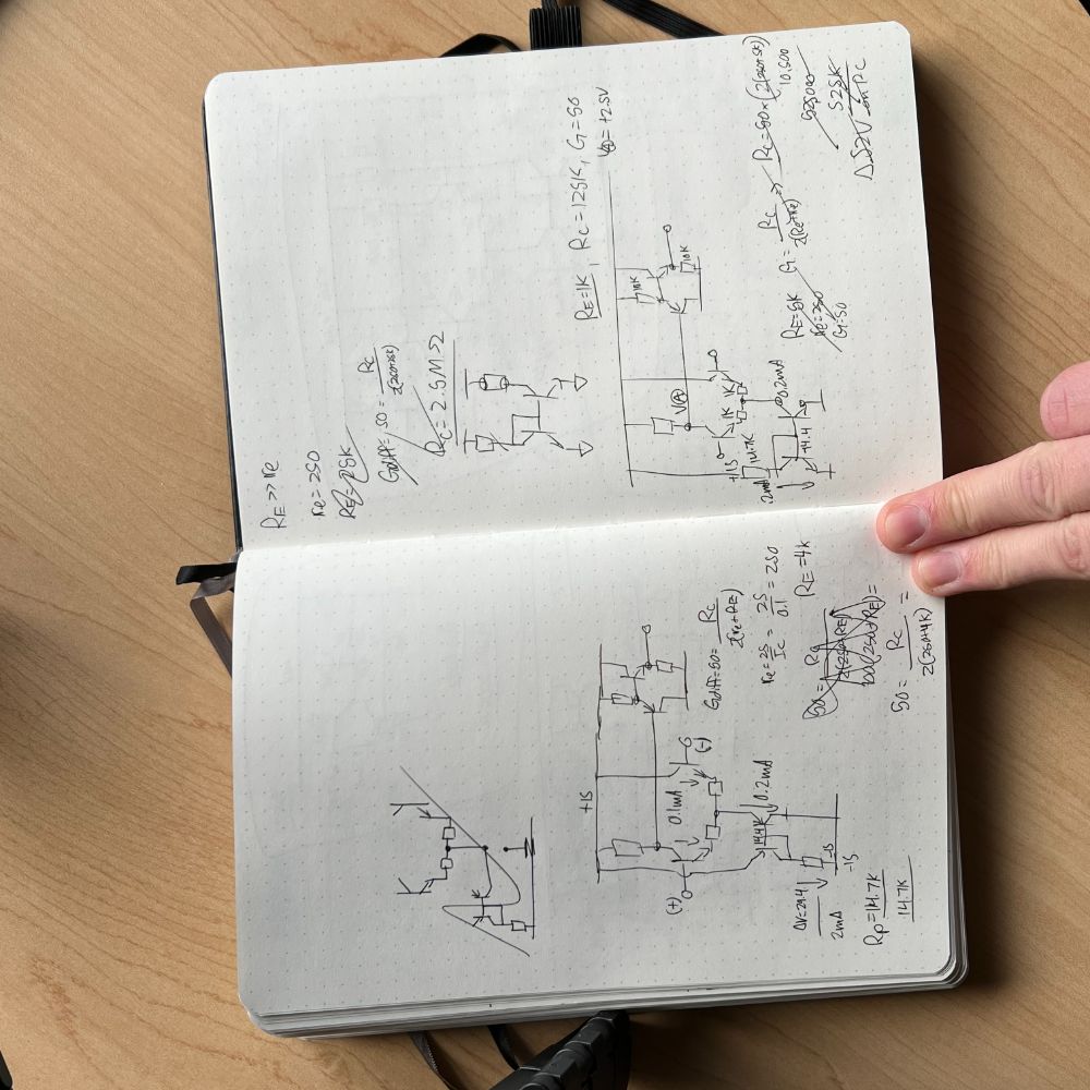
Ex 2.6
zener set to 10V, from a 20-25V supply. load current 0-100mA. zener demands 10mA
what R
what power rating on zener
zener is a shunt regulator
limitations
vout not precise
moderate ripple rejection and regulation against load changes
iwde varying currents require zeners to handle dissipation at low load current levels
Figure 2.21
by strapping an emitter follower to the zener, performance is improved
first, the emitter follower ensures the output voltage is 0.6V lower than the zener setpoint
second, the load the zener sees is now reduced by a factor of B
Just connect the npn to the same power supply as the zener, and now there’s a much better, more regulated circuit, with lower and more consistent power dissipation.
to limit the amount of current going through the transistor, add Rc
make sure the voltage drop across Rc is less than the voltage drop across Rz
That is, make sure the collector doesn’t fall below the base
if the ripple in the zener circuit is still too much you can always just add a lowpass filter to the zener’s bias circuit (R)
2.2.5 – Emitter follower biasing
Notes
If the emitter follower is being driven by an earlier stage in the circuit, they’re probably sharing a power supply.
If they’re sharing a power supply, it’s usually okay to simply connect the output of the prior stage directly to the base of the emitter follower.
One issue where this doesn’t work is if the signal coming into the base is capactively coupled.
Signals that are capacitively coupled have an average value of 0V (no DC Offset) and so swing negative. For the typical emitter follower stuck between Ground and +VCC, this means that the entire negative half of the swing is going to get clipped
The first and fastest way around this is to simply set up a voltage divider at the base, and then connect both the base and the capacitvely coupled signal together in the middle of the voltage divider. This will set the new zero-point of the signal to the midpoint between Ground and VCC.
This process of selecting the characteristics of the circuit when there is no signal being applied (Zero-Point of the signal) is called Quiescent Point
In most cases, the Quiescent Point is chosen to allow maximum symmetrical signal swing of the output waveform without clipping
However, because we’ve effectively added another module to our emitter follower, we now need to consider terminal impedances
The output impedance of the voltage divider should be small, compared to the input impedance of the emitter follower
The essence of selecting these impedances can be boiled down to:
The current flowing in module A should be much higher than whatever is drawn by module B
And the main advantage of the emitter follower is that it can pass a signal while drawing very little current for itself. It’s input impedance is extremely high (B*Re)
R1//R2 << B*Re
A – Emitter follower design example
Now to put this all together
We want to design an NPN emitter follower.
We want it to receive an AC coupled signal.
We want it to pass out an AC coupled signal
The signal will be an audio signal with frequencies [20Hz-20kHz]
VCC is +15V
Quiescent Current is 1mA
The structure is an input signal capacitor joined with a biasing voltage divider, feeding the NPN emitter follower, whose output is then also capacitively coupled to the next stage
The process is as follows
1. Set bias point to 50% of VCC
This part is easy. VCC is 15 so we want the bias at 7.5V.
Note that the bias point refers to the output voltage, not the input voltage
Since the emitter is at 7.5V, the base must be 1D higher at 8.1V.
2. Choose an Re value to create the Quiescent Current called for using that 50%
Since the emitter is at 7.5V, the base must be 1D higher at 8.1V.
To get 1mA from the output voltage at 7.5V, we want 7.5kR
3. Choose Divider Values (note Base current draw makes divider imperfect)
Assuming a Beta of 100, the quiescent current draw into the base should be 10uA.
Recall the loading criteria from earlier. The current drawn by the base should be much lower than the current flowing through these divider resistors
More specifically, the parallel resistance (output impedance) should be at least 10x smaller than the input impedance of the emitter follower.
Since we have selected Re already, and assumed a Beta, it’s easy enough to say that the input impedance into the emitter follower will be 7.5k x 100 = 750k.
The parallel resistance should thus be 1/10 of that, 75k.
At this point, we have that the voltage divider should output 8.1V and that their parallel resistance is 75k. Calculating their values is tedious but trivial.
If they were 50-50 and equal, then their ratio would be 1.
In this case, the first resistor drops (15-8.1)V and the second drops 8.1V
so 6.9 and 8.1
The current flowing through them is usually equal, but not exactly in this case, since some small current is getting pulled into the npn base. this means that the second resistor has less current in it than the first resistor. We have designed this so that that difference in current is trivial though, so we can ignore it and assume they’re still equal.
now, assuming the currents are the same in both resistors, we can safely assume that the ratio of the voltage drops is also the ratio of the resistances.
The ratio is 1.17
Now, we can set up a parallel resistance equation with the upper resistor as X and the lower resistor as 1.17*X, all set to 75k
we get about 130k and 150k
4. Choose C1 to set a high pass filter with its load
An RC high pass filter looks like a capacitor and then a resistor. In this case, we have a capacitor at the input terminal, and then a complicated circuit that can be reduced to a simple resistance. This high pass filter will determine what signals enter the module so it’s highly relevant to make sure we don’t muck up our signal before it goes anywhere
Because the node the capacitor is connected to can flow to both the voltage divider AND the emitter follower at once, we treat their impedances in parallel.
we’ve already determined that the impedance looking both out and into the voltage divider is simply the parallel of the two resistances. that’s 75k.
we’ve also already determined the input impedance into the emitter follower. that’s 750k.
Putting 2 and 2 together, we get a parallel impedance of 75k/750k = 68k
Now we can abstract away this circuit and work on our high pass filter
We know that this RC HPF is an incidental consequence of us capactively coupling the input signal into the circuit, so we don’t want it to attenuate any of our input signal.
Which means we should make sure the entire range of it is after the highpass 3dB point
Our input range is 20Hz to 20kHz, so let’s set the corner frequency to 15Hz to be safe.
From here, we can use the f=1/(2*pi*R*C) formula and solve for C, since we already have f and R.
C = 0.15uF.
5. Choose C2 to set a high pass filter with the output load
Since C2 is forming a second HPF with the output, we consider the load’s value
We’re already assuming that the load will always be bigger than Re
So, for a minimum load value of Re, we can calculate C2 using the same frequency as before, 15Hz
Note that for higher load values, the corner frequency will actually go further down below 15Hz
Also Note that for cascaded high pass filters like this, both capacitor values should be increased slightly to compensate for the increased attenuation
6. Output impedance
Finally, with all values set, we can calculate the final output impedance of this entire circuit
From the output node, there are three paths:
1. Unconnected output to load through C2
2. Ground through Re
3. Ground through npn (through R1, R2, and Source)
Putting this together, the output impedance must be the emitter resistance in parallel with the 1/B factored triple parallel resistances of the two voltage divider resistances and the output impedance of the source that drives this circuit, which we can assume a value of 10k for.
Zo = (Re) // (1/B*[R1//R2//Zin])
A few principles from this example:
The Base-Emitter Junction can be treated as a viable path to ground when calculating input and output impedance
However, if you pass through it, a factor of B will be applied.
If you move from emitter -> base, then everything on the base side needs to be factored by 1/B, from the emitter’s perspective
Similarly, if you move from base -> emitter, then everything on the emitter side needs to be factored by B, from the base’s perspective
Voltage Dividers can be used to bias emitter followers, but they will become imperfect, since some gate current needs to be drained away from R2 and into the base.
This imperfection can be more or less ignored as long as the current running through the divider is ordered higher than the base current
capacitive coupling on both input and output can result in cascaded/stacked filters, which should be treated with caution. f=1/2piRC is essential.
When biasing an AC coupled signal, bias the base to ensure the emitter is at 50%VCC after the 1D drop
B – Followers with split supplies
Another way to get around having to do all this biasing nonsense and just pass a signal through an emitter follower is to have split supplies. That is, a positive and a negative supply rail.
Since AC signals are usually “near ground” and have no DC offset, connecting the emitter to a negative supply instead of 0 gives the emitter follower some negative range to work with.
Warning: base current path to ground
most circuits will assume that the signal source going into the base of the npn will have its own path to ground.
Either way, best practice is still to provide one. This usually takes the form of a resistor connecting the base to ground.
This discussion is relevant when there are symmetrical supplies, because the emitter doesn’t have a connection to ground. Before the base current could go through the BE junction and find its way to ground, but with symmetrical supplies the base needs it’s own path to ground
Perceptive Moment: now the signal/input current moving into the base has two pathways to divvy up current into. It’s easy enough to see that Rb and B*Re are the two options, and so, set Rb to be 1/10th of B*Re
C – Bad biasing
If resistances get multiplied by B when passing through BE anyway, can’t you just set up a voltage divider by strapping a resistor from VCC to B that is 10x the resistor from E to GND?
eg. 750k -> VCC-Base
7.5k -> Emitter-GND
This assumes a value of 100 for the Beta. This circuit only properly divides the voltage and sets the quiescent point at 50% VCC if beta is 100.
Beta changes from transistor to transistor and on the temperature and on what color socks the president is wearing today. Relying on it and designing your circuit around it is a recipe for disaster. Don’t do it.
Using a stiff voltage divider makes the quiescent point of the circuit independent of fluctuations in Beta.
D – Cancelling the offset – I
a PNP emitter follower is similar, but since the arrow is pointing inwards and the emitter is on top and expected to be more positive,
the collector is on the bottom of the symbol and connects directly to ground. the emitter is on top of the symbol, points in towards the base, and connects to VCC through the emitter resistor.
In this case, the emitter follower is on and active as long as the base is 1D LOWER than the emitter.
Meaning that the output of the PNP emitter follower, at the emitter terminal, is 0.6V higher than the input signal.
So if you just put two of these together, PNP then NPN and match the emitter resistors, no problem. Offset Cancelled (RIP Offset)
Note that if you don’t have symmetrical supplies, you’re still going to experience negative side clipping despite the cancellation
note that Vbe varies with a number of things and this will be slightly imperfect. If you need perfect, use an opamp
2.2.6 – Current source
A – Resistor plus voltage source
You can make a current source by using a voltage source and a resistor in series with the load terminal
The only thing is, the voltage has to be huge and the source resistor has to be huge, so huge that the addition of the load resistance is trivial.
That is Rs+Rl =~ Rs
This source resistor also experiences large power dissipation, which is another issue
Note that when dealing with voltage sources, we talk about loads in terms of the current they’re going to draw
when we are dealing with current sources, we talk about how much load voltage instead
Since after all, for a constant current, the bigger the load resistor, the higher % of the total resistance between source and load resistance it’ll occupy, and thus the more voltage drop it’ll take
Ex. 2.9
if you wanted a current source to remain constant within 1% over a load range of 0-10V, that is a different way of saying, how big does a voltage source need to be for a 10V fluctuation to account for less than a 1% change?
1000 Volts, across a 1K source resistor, results in a 1A current
If another resistor is added such that the 1K source resistor now takes 990V and the load 10V, the current will decrease from the added resistance
It’s easy enough to calculate what this new reduced current will be since we already have the voltage drop across a known resistor: 990v/1000r = 0.99A. a 1% reduction in amperage for a 10V load
B – Transistor current source
Due to a supply shortage of 1000V power supplies and 1kW resistors, we have had to come up with alternative methods for sourcing stable currents (this is a joke)
It’s much easier to make a current source out of a transistor.
take an npn, give its base a voltage, calculate the 1D drop to the emitter, run a resistor from the emitter to ground
Picking the input voltage and the emitter resistor sets the current flowing out of the emitter
Technically, Ie=Ib+Ic, but in this case we can say Ie=Ic as long as the beta is high enough. a 100 Beta means the difference between Ie and Ic is only 1%
From there, we can just attach our load between the VCC and the collector. The current flows through the load as determined by our transistor/emitter resistor and voila.
C – Current-source biasing
So now we just have the problem of how to set that voltage.
Can we use a voltage divider again? yea sure
Remember to keep it STIFF. that is, the output impedance of the voltage divider needs to be small compared to the input impedance of the current sourcing transistor circuit.
Remember the triangle |>: small output impedance, large input impedance
for a voltage divider, the output impedance is always just the two resistors in parallel.
For the npn, the input impedance is B*Re. (remember there is no meaningful path through base-collector, so our load does not factor in here!)
There are other fun ways to set the voltage too, like using a zener, or even just stacking Diodes until the N*1D is where you want it
D – Compliance
Current sources can only provide constant current for some range of load voltages.
An earlier example could range between 0V and 10V for the load voltage and keep the current accurate to within 1%.
For these simple transistor current sources, the main criteriea is that the transistor remain in the active region.
This is qualified by the Collector being at least 0.1V above the emitter.
in 2.32A, the emitter is at 1.0V, so the collector has to be 0.1V above that. the lowest voltage the collector can go to is them 1.1V.
VCC in this case is 10V
If there were no load and the collector could connect directly to VCC and the VCE would be 10->1 = 9V
As the load varies, the voltage drop across the load can increase or decrease, but that voltage drop can’t expand so much that the collector drops below 1.1V.
This means that the maximum load voltage is 10-1.1=8.9V.
So this current source is COMPLIANT for [0-8.9V] and will provide approximately constant current for all loads in that voltage range
In the event that the load has its own supplies or batteries or sources or what have you, it can actually act as a voltage source that INCREASES the voltage at the collector. This is fine for the most part, but every transistor will have a maximum Collector-Emitter breakdown voltage.
E – Cancelling the offset – II
you can use the same PNP-NPN emitter follower offset cancellation structure here in the current source as well.
After all, the only difference between an emitter follower and a current source is
a load connected between VCC and the Collector
The emitter takes in and passes an input signal, the source doesn’t
one is POWER, the other is CONTROL oriented
This makes it simple and clean
Vin is approximately equal to emitter voltage on Q2. So you just set the second emitter resistor and input voltage and the load will see that current. It’s as easy as I=V/R now
F – Deficiencies of current sources
It’s not perfect, but it’s better than looking for the fabled 1kW resistor
2.2.7 – Common-emitter amplifier
Notes
As mentioned previously, the Emitter follower is a CONTROL type circuit, which takes in and passes out a signal
The current source is a POWER type circuit, which supplies energy, but doesn’t deal with signals or information really
We are now going to combine them
This combination of both power and control characteristics is called the Common-Emitter Amplifier
to begin with, take the classic transistor current source, and give it a load resistor.
Next, we are going to capacitively couple a signal into this current source at the base.
But in order to do this, we’ll also need to add a voltage divider for biasing.
At this point, we have the transistor with its emitter resistor, a collector resistor acting as a load, two resistors forming a voltage divider on the base, and then a capacitor for coupling the input signal.
Since this is intended to act as a current source, we don’t actually want to bias it to 50%VCC. The output isn’t the emitter terminal anyway, it’s actually the collector. More on this in a moment
The collector’s voltage isn’t related to the base or emitter voltages so directly as a 1D drop.
We can see that the voltage at the collector terminal is just VCC subtracted by whatever voltage gets dropped through the collector resistor
That is
Vc = VCC – Ic*Rc
VCC is known, and so is Rc, since we picked it already
Only thing left is Ic
We can assume a high Beta and that Ie=Ic.
Thus, since Ie = Ve/Re = Ic,
We can bias the base, set Ve, and then pick Re to set the emitter current, which is also the collector current
Now to actually Bias it.
Use this ability to set the Ic and Rc to put the collector at 50%VCC
Now the stage is set.
We inject a wibbling signal in via the input capacitor, causing the base voltage to wibble.
The rule is that Ve is always 1D lower than Vb while active, and this wibble is small and doesn’t deactivate the transistor.
This means that Ve also matches the wibbling of Vb
And if Ve is changing, that means that the current going through Re is also changing.
And since the emitter current is equal to the collector current in this case, that means the voltage drop across the collector resistor is wibbling too.
Finally, the Collector voltage is wibbling.
It’s worth noting though, that since for Vc to go UP, the collector current has to go DOWN (reducing the voltage drop in the collector resistor and bring the collector terminal closer to VCC),
The relationship is negative. That is, the signal comes out flipped upside down
Derivation of the same
vb=ve
ie = ve/Re
ie = vb/Re
ie = ic
ic = vb/Re
Vc = VCC – Ic/Rc
vc = -ic/Rc
ic = vb/Re
vc = -(vb/Re)*Rc = -vb*(Rc/Re)
vc = output
vb = input
vc/vb = Gain
vc/vb = -Rc/Re
Gain = -Rc/Re
This is called a
Common-Emitter Amplifier with Emitter Degeneration
A – Input and output impedances of the common-emitter amplifier
The most important concept here is remembering that there is no meaningful path from collector to base. the resistance is measured in the megaohms
To summarize
Base -> Emitter: multiply by B
Emitter -> Base: divide by B
Base -> Collector / Collector -> Base: A brick wall
Collector -> Emitter: this path routes through the Base ergo, Brick Wall
Input Impedance
Signal comes in, sees three paths to ground
1 through R1
1 through R2
1 through the BE junction and down through Re
Thus, Zin is R1//R2//B*Re
Output Impedance
From the output, two paths to ground
1 through Rc
1 through the brick wall (Megaohms)
Since they’re in parallel, we ignore the brick wall and say it’s just about Rc.
Note that the output impedance for the common emitter amplifier is determined by the collector load resistor
The emitter follower from earlier’s output impedance was determined by the parallel paths of Re and (1/B)*[everything on the input side].
Since the 1/B side is almost always much lower then Re, the output impedance of the emitter follower is independent of the emitter resistor (load resistor for the ef)
Output Impedance
Common Emitter Amplifier
Dependent on Load Resistor (Rc)
Emitter Follower
Independent of Load Resistor (Re)
2.2.8 – Unity-gain phase splitter
Notes
A phase splitter generates a signal and its inverse, the upside down one.
The common emitter amplifier by default only puts out the inverse, but it’s possible get the upright one out of it
First, set the gain to unity by making the collector and emitter resistors exactly equal.
Now, the voltage drop across both of Rc and Re will be equal
Meaning the signal measured at the collector will be the upside down one, but the signal measured at the emitter terminal will be the right side up once, since it’s being measured from ground
also note that if you were to measure VCC with the collector output as the REFERENCE (GND) you’d see the upright signal. but this isn’t meant to inform design decisions. Just reminding you that everything is relative to a reference point
Now that the phase splitter is active, we want to bias it carefully so that both signals have enough room to swing without clipping or slipping the transistor into saturation.
If you have a signal that goes up and down, then you want the quiescent point collector voltage at 0.75VCC, so that it can stretch 0.25VCC in either direction, to 1.0VCC or 0.5VCC
Since the voltage drops will be the same, this also means that the emitter terminal will rest around 0.25VCC and then fluctuate up to 0.5VCC or down to 0
A – Phase shifter
This part is black magic
Since we have two signals, and they’re the inverse of eachother, if you were to measure the difference between them, you’d just get a double amplitude version of the signal
but if instead, we bridge the two signals with an RC, and measure the middle voltage, we’ll find that the new output is the same signal, with the same amplitude, but phase shifted by
theta = 2*atan(w*R*C)
And so we replace R with a potentiometer so we can change the angle of the phase shift
R=0 -> theta=0
cue phasor diagram
V+ and V- form unit vectors that point in opposite directions, forming a line of length 2.
Vc and Vr are vectors that travel from the tip of V+ to V-, and are required to be at right angles.
Note that Vc is flexible as well as Vr, since it’s not Xc, but Vc. R can dominate the voltage drop and leave little left for C. Vc can shorten.
Finally, this technique is useful but a little crude due to loading effects. the resistor can’t get too big. Later on, there will be improved phase splitter effects using Opamps
2.2.9 – Transconductance
Notes
There were a few steps to the common emitter amplifier
a
applied base voltage wibble results in an emitter voltage wibble
b
calculating emitter current, ignore base, determining collector current
c
calculating the collector voltage swing
The amplifier can be broken into two sections
First Section: everything but the collector resistor
the INPUT is the base voltage
the OUTPUT is the emitter current
Thus, the GAIN = OUTPUT/INPUT
GAIN has units of Current/Voltage
I/V = 1/R, thus the units are CONDUCTANCE
therefore, the first section is a TRANSCONDUCTANCE Amplifier
In this case, the gain is just -1/Re
If Re is 1k: you can input 1V and you’ll get 1mA
That is, I(V) = (1/Re)*V
I(1.0V) = (1/1000[A/V])*(1.0V) = .001A
transconductance gain is “gm”
Second Section: the collector resistor
the INPUT is the collector current (equal to emitter current)
the OUTPUT is the collector voltage
Thus, the GAIN has units of Voltage/Current, which is Resistance
V/I=R, Thus the units are RESISTANCE
therefore the second section is a TRANSRESISTANCE Amplifier
In this case, the gain is Rc
V(I) = Rc*Ic
V(1mA) = (10,000)*(1mA)
V(1mA) = 10V
transresistance gain is “rm”
And so the transconductance section converts a voltage to a current
and then the transresistance section converts a current back to a voltage
overall gain is the product of the two gains
Gv = gm*rm
Gv = -1/Re * Rc = -Rc/Re
You can analyze them separately as well, replacing transconductance circuitry with a different circuit topology with a similar value of gm
You can also change the load part and check gain versus voltage swing, there are tradeoffs there as well.
An active load/current source can have a transresistance of 10,000V/A or more
A – Turning up the gain: limitations of the simple model
If you reduced Re, the -Rc/Re would imply that gain would rise without limit at Re -> 0 but that doesn’t happen. Cue Eber Molls
B – Recap: the “four topologies”
So far, we’ve seen 4 circuits
Transistor Switch
Switch: no emitter resistor, load on collector
Emitter Follower
Control: no collector resistor, emitter resistor to set current, output on emitter
Current Source
Power: emitter resistor to set current, collector on load
Common Emitter Amplifier
Power+Control: emitter and collector resistors, output on collector
2.3 – Eber-Moll model applied to basic transistor circuits
2.3.1 – Improved transistor model: transconductance amplifier
Notes
For many applications, there is no need for an advanced model of the BJT
Switch, Current Source, Follower, Amplifier
Now it is time to dive deeper
The previous model of the BJT was as a current controlled current source
That is, current in, current out
Ic = B*Ib, to be specific
Input, Ib, Output, Ic
Now we’re looking at it as a transconductance device:
Voltage in, current out
Ic as a function of Vbe
The applications for this more specific modeling include
differential amplifiers
logarithmic converters
temperature compensation
etc
all fancy higher precision analog stuff
NEW RULE #4
When rules 1-3 are obeyed, the following relationships are true:
Vt = kT/q
Ic = Is(T) * [e^(Vbe/Vt) – 1]
Vbe = Vt * ln[ (Ic/Is(T)) + 1]
notes
The current passing through the collector
Is a scaled version of Is(T)
Is(T) is the saturation current, which varies from transistor to transistor, and also varies by temperature
the scale factor is e raised to the power of the ratio of the base emitter voltage to the ambient thermal voltage
Thermal voltage is the ambient voltage present in the transistor at a given temperature, and Vbe gets ratio’d by that in order to determine how much current passes through
Vt – Thermal Voltage
q – electron charge constant
1.60×10^-19 C
k – Boltzmann’s constant
1.38×10^-23 J/K
T – absolute temperature
K
Old Rule #4 (pre-Ebermolls)
If 1-3 are followed
Ic is proportional to Ib
Ic = B*Ib
B is Beta which is h_fe
“h parameter transistor model” is no longer popular
New Rules
NPN Rules (reverse for PNP)
1 – Polarity
Vc must be greater than Ve
2 – Junctions
Base->Emitter and Base->Collector act like diodes
Base->Emitter diode is usually conducting
meaning base is higher than emitter by at least one diode drop
Base->Collector diode is usually reverse biased
current can’t flow into the base from either E or C
Control current flows into B and out through E
3 – Maximum Ratings
All transistors have max values for
Ic – current flowing through collector-emitter
Ib – current flowing into base
Vce – voltage across collector-emitter
exceed them and it breaks
Other limits worth noting
Max power – Ic * Vce
Max Vbe
NEW RULE #4
When rules 1-3 are obeyed, the following relationships are true:
Vt = kT/q
Ic = Is(T) * [e^(Vbe/Vt) – 1]
Vbe = Vt * ln[ (Ic/Is(T)) + 1]
notes
The current passing through the collector
Is a scaled version of Is(T)
Is(T) is the saturation current, which varies from transistor to transistor, and also varies by temperature
the scale factor is e raised to the power of the ratio of the base emitter voltage to the ambient thermal voltage
Thermal voltage is the ambient voltage present in the transistor at a given temperature, and Vbe gets ratio’d by that in order to determine how much current passes through
Vt – Thermal Voltage
q – electron charge constant
1.60×10^-19 C
k – Boltzmann’s constant
1.38×10^-23 J/K
T – absolute temperature
K
Old Rule #4 (pre-Ebermolls)
If 1-3 are followed
Ic is proportional to Ib
Ic = B*Ib
B is Beta which is h_fe
“h parameter transistor model” is no longer popular
Vt = kT/q
Ic = Is(T) * [e^(Vbe/Vt) – 1]
Vbe = Vt * ln[ (Ic/Is(T)) + 1]
Note that in the transistor’s active region, Vbe >> Vt, and so the result of the exponential becomes high enough that the -1 can be ignored in the formula for Ic
Ic = Is(T) * e^(Vbe/Vt)
The value that determines the collector current is actually base-emitter voltage
Beta was just a rough approximation
this new formula is also accurate over a wide range of currents, nA to mA.
If you map the actual Ic vs Beta, that’s called a Gummel Plot
Typical Gummel plots look like a wide flattish hill, meaning Beta decreases at extreme ends. It’s most stable from 10^-7 to 10^-2 A
Or, 100nA to 10mA – stable beta range
2.3.2 – Consequences of the Emers-Moll model: rules of thumb for transistor design
Notes
Some simple and handy “Ratio Rules” to help calculate changes in Vbe and Ic
Ratio Rule #1 – Change in Vbe
Ic2/Ic1 = e(dVbe/Vt)
the ratio of the new current over the old current
is equal to the exponential of the change in Vbe divided by Vt
Ratio Rule #2 – Change in Ic
dVbe = Vt*ln[ Ic2/Ic1 ]
the change in base-emitter voltage
is equal to the natural log of the ratio of the new current and the old current, scaled by the thermal voltage
A – The steepness of the diode curve.
using these ratio rules, it’s easy to derive that, to 10x collector current, we only need to increase Vbe by ~60mV.
Four More Shorthands
1
10xIc -> dVbe = +60mV
2
2xIc -> dVbe = +18mV
Ic doubles every 18 mV
3
4%dIc/1mv
every mV increases Ic by 4%
4
Ic = Ic0 * e^(dVbe/.025)
dVbe in Volts
B – The small-signal impedance looking into the emitter, re, for the base held at a fixed voltage.
now to do something awful and take the derivative of one of these formulas
Vbe = Vt * ln[ (Ic/Is(T)) + 1]
we’re going to calculate the derivative of Vbe with respect to Ic
That is, if the base voltage is constant, how do Ic and Vbe influence eachother?
dVbe/dIc = will also be units of incremental Resistance, dR
actual math
by doing a u-substitution and natural log derivative, you’ll get
[Vt + 1/Is] / [(1/Is * Ic) + 1]
We can assume the +1 is irrelevant
and then we can cancel the 1/Is
We’re left with
Intrinsic Emitter Resistance – re
re = Vt/Ic
Where Vt at room temperature is usually 25mV so either
re = 0.025/Ic (Ic in Amps)
or
re = 25/Ic (Ic in mA)
Note that this formula can be inverted and instead of representing resistance it can represent conductance
gm = Ic/Vt
if in mA and mV,
gm = 40*Ic
C – The temperature dependence of Vbe.
Even though the Vbe equation scales directly with temperature,
Is(T) scales with temperature inversely, stronger than that
To the point that Vbe actually decreases with temperature overall
Handy Rules
at constant Ic, Vbe decreases 2.1mV/C
at constant Vbe, Ic increase about 9%/C
D – Early effect.
at constant Ic, Vbe varies slightly with changing Vce
dVbe = -N*dVce
N usually around .0001 to .00001 (10^-4 to 10^-5)
Ic = Ic0 * (1 + Vce/Va)
Another way to express it is in terms of Early Voltage Va
Early voltage comes from this expression
N = Vt/(Va+Vce)
which then simplifies to
N = Vt/Va
2.3.3 – The emitter follower revisited
Notes
To summarize all of the changes and finnicky interdependencies:
Formulas:
Vt = kT/q
Ic = Is(T) * [e^(Vbe/Vt) – 1]
Vbe = Vt * ln[ (Ic/Is(T)) + 1]
Ic = Is(T) * e^(Vbe/Vt)
Four More Shorthands
1
10xIc -> dVbe = +60mV
2
2xIc -> dVbe = +18mV
Ic doubles every 18 mV
3
4%dIc/1mv
every mV increases Ic by 4%
4
Ic = Ic0 * e^(dVbe/.025)
dVbe in Volts
Handy Rules
at constant Ic, Vbe decreases 2.1mV/C
at constant Vbe, Ic increase about 9%/C
Early effect
at constant Ic, Vbe varies slightly with changing Vce
dVbe = -N*dVce
N usually around .0001 to .00001 (10^-4 to 10^-5)
Ic = Ic0 * (1 + Vce/Va)
Another way to express it is in terms of Early Voltage Va
Early voltage comes from this expression
N = Vt/(Va+Vce)
which then simplifies to
N = Vt/Va
Intrinsic Emitter Resistance – re
re = Vt/Ic
Where Vt at room temperature is usually 25mV so either
re = 0.025/Ic (Ic in Amps)
or
re = 25/Ic (Ic in mA)
or
gm = Ic/Vt
if in mA and mV,
gm = 40*Ic
Summary
Vbe now determines Ic
Beta is still in play
increasing Vbe increases Ic
constant T
increasing temperature decreases Vbe
constant Ic
increasing temperature increases Ic
constant Vbe
increasing Vce decreases Vbe
constant Ic
Increasing Vce increases Ic
constant Vbe
add an intrinstic resistor in series at the emitter
re = Vt/Ic
Generally speaking, we just say re = 25 @ 1mA
re = 2.5 @ 10mA
re = 250 @ .1mA
and so on
The source impedance of the emitter node specifically (with fixed base voltage) will just be the change in Vbe wrt to the change in Ie
But since Ie ~ Ic
dVbe/dIc = re = Vt/Ic = 25/Ic
The source impedance of the emitter node specifically is re
The reason the emitter follower has sub-unity gain is because the intrinstic emitter resistance forms a voltage divider with the load, and eats up some of the voltage on the way down
Eber Molls effect on the Input and Output Impedance of the Emitter Follower
Since there is now a tiny resistor attached to the emitter, any load connected to the emitter will be forming a voltage divider between re and RL
Output/Source Impedance
2 parallel Paths to ground from the output node (unloaded)
1
through RE
2
through re, bjt, source resistance, voltage source
Meaning the overall output impedance can be expressed as
Zo = RE // [re + (1/B+1)*Rs]
Input/Load Impedance
From the input node, the signal passes through the BJT
Then through the intrinsic emitter resistance
From there, there are two paths to ground, RE and RL
So, the overall input impedance is
Zi = (B+1)*[re+(RE//RL)]
2.3.4 – The common-emitter amplifier revisited
Notes
If the common emitter amplifier has an emitter resistor
this is called “Emitter Degeneration”
Which is pretty dramatic terminology for something that just reduces the gain a little in exchange for stability
Recall that gain for the common emitter amplifier was
Gv = -Rc/Re
now we know that Re will never be zero, but will at least be re = 25mV/Ic[mA]
this means that the gain will fluctuate like crazy with output current.
If we add a large resistor to drown out the re, like 1k or 10k, the gain will obviously go down, but it will remain stable for a larger range of currents
So as long as there’s the external emitter resistor present, we can usually just ignore re
There is another case though where you parallel the RE with a capacitor
Now, high frequency signals can ignore RE and go straight to ground, which means they’re concerned primarily with re.
That also means that re will form an RC filter with the RE-parallel capacitor
If we have a common emitter amplifier, without an emitter resistor, we will not have infinite gain
Similarly, if we measure the input impedance, we know that it’s not zero now, because that tiny re is there.
Zin is now going to be (B+1)*re
“common emitter” and “grounded emitter” are sometimes used interchangeably, to refer to when there’s no external emitter resistor. RE = 0
the “common” means ground. more specifically. the input and output share the same ground
base and emitter, share the same ground
and they both have a path to ground
the collector, no path to ground
A – Shortcomings of the single-stage grounded emitter amplifier
1. Nonlinearity
Simple 10k Collector resistor, no emitter resistor
Gv = -Rc/Re
Re = re = 25/Ic
Gain varies from -800 down to zero between 2mA and 0mA
Awful performance
Poor linearity, tons of distortion
This thing could be useful with some feedback
Without feedback, it’s only useful for small signal swings around the Q point
ONE MORE TIME
The emitter degenerated common emitter amplifier
Adds Re >> re
Such that the gain becomes effectively independent of Ic
Incremental Gain & Distortion & Nonlinearity
Several new concepts here on the grounded emitter amplifier
First
Incremental Gain
The quiescent gain is
Gv = -Rc/(25/Ic_q)
Where Ic_q is the quiescent current
Flipping this around we get
Gv = -Rc*Ic_q/25
the 25 is Thermal Voltage, Vt
and Rc*Ic is just Vrc – the voltage drop across the collector resistor
In this case, we’re specifically talking about the quiescent voltage drop
Obviously, the voltage drop across the collector resistor will change with collector current, etc.
Gv = -Vrcq/Vt
Now we can say that the gain is equal to the ratio of the voltage drop across the collector resistor, to the thermal voltage
Now, for incremental gain
Since Vrc is variable, we can say this is a function
Gv(Vrc) = -Vrc/Vt
and so the incremental gain dGv is determined per volt of dVrc and the 1/Vt factor
dGv = -dVrc/Vt
Nonlinearity
Nonlinearity can be quantified as the fractional change of gain with swing
fractional change of gain referring to gain increasing by 10% or something proportional like that
These changes in gain are proportional, so they’re referenced back to the quiescent Gain, so
(Ginst – Gq)/Gq
and swing referring to the distance between an instanteous voltage and the quiescent voltage
Since after all, signals push voltages up and down and move it away from the quiescent point. This distance from Vq is referred to as swing.
Specifically, instantaneous swing
But it’s not just the raw voltage difference, it’s also fractional, referred back to the quiescent voltage drop
That is, swing is (Vinst-Vq)/Vq
Also expressed as dVout/Vdrop in the book
Putting this together, we get our expression for nonlinearity:
dG/G = dVout/Vq
Distortion
Finally, distortion
If distortion is present, that means the signal is not perfectly linear
A perfectly linear signal has no distortion
Therefore, the measure of distortion is to take the waveform, subtract the strictly linear part, and whatever is left is the distortion
the amplitude of whatever is left is the quantity of distortion, and we measure that as a fraction of the total amplitude of the waveform.
Meaning we might get numbers like 5% distortion
For some reason I do not understand, we divide the number by 3 and say that’s the distortion
so 1.66% distortion if you calculate 5
It’s important to be clear, nonlinearity and distortion are two different ways of talking about the same thing in this context.
That is, to calculate distortion, just solve the dG/G from earlier
If gain moves from 200 to 204, you can calculate distortion right then and there
(204-200)/200 = 4/200 = 2%
2/3 = 0.7
0.7%
Even adding just a 225R resistor to the emitter will drastically improve linearity.
It comes at the price of reducing quiescent gain by 10x though
Example, given a fluctuating triangle input, you can calculate gain
use the input voltage, and our rule of thumb of +4% IC per 1 mV+
IC Changes, the voltage drop across Rc changes, and from there gain can be calculated
a simple 10V supply, 5V output bias, 5k resistor circuit being fed a 25mV triangle wave is going to have its gain flying all over the place
>20% distortion and such
2. Input Impedance
Because the signal source impedance and the amplifier’s input impedance form a voltage divider, the grounded emitter amplifier will experience further nonlinearity
if the emitter is directly grounded, then
Zin = B*re = B*25/Ic
3. Biasing
You might think you can use the eber molls equation to bias the grounded CE amp (GCEA) to some fine tuned Vbe,
But since Vbe is roughly proportional to 1/T, that means even small changes in temperature will cause the transistor to saturate.
fixed Vbe, Ic rises 10x for a 30C temperature rise
Vbe: 2.1mV/C
Ic: 9%/C
Ic: 10x / 30C
B – Emitter resistor as feedback
The transistor is a TRANSCONDUCTANCE DEVICE
Gain is in terms of A/V
Input is a voltage, output is a current
Input into the amplifier is Vin, measured from Ground
AKA Vb
Output is collector current Ic
We convert this current back into a voltage using a Transresistance device, a resistor
it converts current into voltage, and then we measure the voltage and back-calculate the current using the gain of the transresistance device (resistance of the resistor, measured in Volts/Amp)
Negative Feedback involves taking some portion of the output and feeding it back into the input
It costs some gain to have but improves many characteristics like linearity
adding an emitter resistor is a form of negative feedback
Input is VB, but that’s not what fully determines IC
What fully determined IC is VBE
Which is VB – VE
This means the input is modified, it’s subtracted by some term VE
But VE is not a static value
VE actually changes according to the output, IC – making it a sample of the output
What’s more, the emitter resistor actually serves the same tranresistance conversion role as the collector resistor.
The collector resistor converts the output current into an output voltage that’s easier to measure and pass around
the emitter resistor converts the output current back into a voltage so that that sampled voltage can then be subtracted from the input, VB in the form of negative feedback.
The circuit diagram may not show a complete loop being formed but negative feedback is present in this circuit, since a portion of the output is fed back into the input.
2.3.5 – Biasing the common-emitter amplifier – B Start
Notes
If you need high gain and so don’t want to do feedback, there are a few more options
A – Bypassed emitter resistor
Since the amplifier is meant to amplify signals, which are AC and not DC
You can just add a capacitor in parallel to the emitter resistor and then bypass it
the capacitor’s impedance decreases with frequency, so its presence means AC circuits pass through the intrinstic emitter resistance, and then have a free short to ground and can freely ignore the emitter resistor
DC can’t ignore that capacitor and has to go through the emitter resistor
This is useful, because we can have a small emitter resistor providing gain that is high and stable, while still allowing the actual signals to pass through unimpeded. The gain remains high because the voltage at the emitter remains above ground due to the emitter resistor.
You can’t have the emitter voltage too low. Something like 0.2 is too low, because fickle variations in Vbe will cause Ve to fluctuate in dramatic proportion to its total value.
If Vbe climbs from 0.6 to 0.625, Ve will drop 10%, and so will Ie. Not a good situation
Keeping Ve up to around 1V is sufficient for most cases
The whole system is more stable if you use two resistors and add the capacitor bypass for the second one though, forcing the current to pass through the first resistor.
This helps further stabilize Ve, while still retaining the benefits of increased gain at signal frequencies
bypassed emitter resistor means stable biasing without change in gain at signal frequencies!!
1/10th of whatever Vc is a good guideline for Ve
Note that if you’re going to add a bypassed emitter resistor structure like this,
When you go to calculate the input impedance of the amplifier, (for the RC filter formed by the input coupling capacitor and the input impedance of the rest of the amplifier)
you need to do it AT SIGNAL FREQUENCY
Meaning that emitter resistor is getting bypassed and not factored into the signal frequency level input impedance
you can also put 1 R in parallel with an RC series.
The lone R sets the DC bias point
The R in RC lets you set the signal-level gain
B – Matched biasing transistor
Sometimes, you can buy a chip that has two transistors in the same monolithic package
That is, two transistors, one stone.
This means that the transistors will always be the same temperature, and so temperature effects will be negated
I mean, obviously the normal temperature effects are still in play, like overheating it such that saturation occurs. But you don’t have to worry about one transistor getting hotter because it’s moving more power, and then its Vbe and Ic and all that start shifting around, etc.
C – Feedback at dc
You can add a voltage divider at the bases, but instead of connecting it to VCC like a normal person you can be a little freak and connect the top back to the collector
If the emitter is grounded, this means the middle of the voltage divider will for sure be 1D. BUT, if, for example, the divider ratio was 10:1, that means that 1D drops on R2, and then 10x1D drops on R1.
This forces the collector to stay up at ~11x1D with reasonable efficacy
This is cool, but the R1 resistor now serves as a path from the input to the output and so the input impedance is reduced pretty dramatically
D – Comments on biasing and gain
since Gain is
G = -Rc/Re
and the grounded emitter amplifier has just
re = 25/Ic
Why not just increase Ic so the re gets lower, and the gain goes up?
Well, if you want to increase the gain but keep your quiescent voltage
the higher current means you’re going to have to use a smaller resistor for Rc in order to maintain the same voltage drop across Rc
In fact, you can prove that the Gain of a grounded emitter amplifier biased to 0.5Vcc at the collector has a Gain limit of G=20*Vcc independent of quiescent collector current
Exercise 2.16
Design a tuned common emitter amplifier stage to operate at 100kHz. Use a bypassed emitter resistor and set the quiescent current at 1.0mA. Assume Vcc = +15V and L = 1.0mH, and put a 6.2k resistor across the LC to set Q=10 to get a 10% bandpass. Use Capacitive input coupling
First, the layout of the circuit
A Common Emitter amplifier has three zones: the load at the collector, the emitter, and the biasing circuit
the load at the collector is going to consist of an RLC parallel circuit
this RLC will form a bandpass filter
the emitter is going to have a parallel R//RC for the bypassed emitter resistor
one resistor to set the DC bias at the emitter terminal/DC Gain
and an RC to set the gain for signal frequencies
the base is going to have a normal voltage divider for base voltage biasing, and then a standard input capacitor as well
Next, the sequence of approach
There are five areas that need solving
A
Use given R, L, Q, and f to solve for C in the RLC
B
Select a VE, and RE for emitter bias and DC gain
C
Select R, C, and f in the emitter-bypass to pass signal frequencies
D
Bias the base voltage divider and supply ample base current
E
Select Cin by analyzing the overall High Pass Filter formed by Cin and the Input Impedance Zin of the entire circuit
A B and C can all be done first, D has to be done after B, and E has to be done last
If you can do this problem quickly and accurately, you have a good grasp of what’s going on
2.3.6 – An aside: the perfect transistor
2.3.7 – Current mirrors
Notes
A current mirror is easy to make
But you do need a matched transistor
Thankfully, in the world of ICs, matched transistors in single monolithic packages are plentiful
Here’s what you do.
Take a transistor, PNP example
Connect VCC to emitter on top
Connect Resistor through Collector down to ground
Connect Base to Collector
Now base current flows in through E->B, creates voltage drop 1D
Now Base and Collector are both VCC-1D
voltage goes through resistor and makes current IP = VCC-1D/RP
By selecting R we select the current
Now, since we have a matched transistor, and their properties are identical at all times, any Vbe we apply to the second transistor will result in an identical Ic on the other side, Thanks Eber-Molls
So we just connect the Base-Collector node to the base of the other matched transistor
Now all that’s left is to connect a load for the current source to source current through, on the other side.
If we need to change the current, we just change the programming resistor
the second transistor doesn’t get a say in the current, it just samples the Vbe of the leader.
Note, resistor goes on the opposite side of the B-E junction, always on the collector
E straight to supply rail
A – Current-mirror limitations due to the Early effect
Now, we know the VCE for Q1 in the current mirror circuit is just going to be VCC down to 1D.
In this case, 15 -> 0.6V = 14.4V is the VCE for Q1
However, the VCE for Q2 won’t necessarily be the same
Because the current is set, a wide range of load resistances can be selected and the current source will be compliant
But since V = IR, the load resistance and the output current together form the collector voltage, which won’t necessarily be 0.6V.
This means that VCE is liable and almost guaranteed to be different from the VCE in Q1
And we know from the Early Effect that VBE to maintain a fixed current actually changes dependent on VCE
Meaning the currents won’t be exactly equal, but that level of precision is not needed
You can improve the performance of this by adding matching emitter resistors that drop a few 10ths of a Volt or 1V. This negates the effects of small variations of Vbe and Vce on the output current
B – Wilson Mirror
If you pay close attention
In NPN BJTs, the base current flows into the base, and combines with the collector and the sum moves out through the emitter
in PNPs, the emitter points inwards, and contains the sum of currents
Once it enters the emitter, the base current forks off and flows OUT through the base terminal
Where does this base current go?
In the current mirror, the two PNP transistors have their bases connected. Obviously these two base currents don’t just combine and cancel out. They would cease to flow and be currents in that event.
The connection that ties the two bases down to the Q1 collector will be where the two base currents flow out through
meaning, the current seen by the Rp programming resistor is actually higher than the collector current
It’s actually Ic + 2xIb
The load resistor is Ic + 0xIb, so the currents are not equal both due to early effect and due to the base current error
The wilson mirror is a clever solve for this
After the two base currents recombine, just add another transistor before the load resistor, a PNP. This PNP will take one of the base currents from the entrance at the emitter and pass it out through it’s base back over to the top of the programming resistor.
Now the programming resistor is seeing Ic + 1xIb
The current leaving this Q3 new transistor will still have one of the two Ib’s with it, so leaving the collector of the Q3 and entering the load resistor is also Ic + 1xIb
Thus, the base current error is exactly cancelled!
Hooray!
Note that Q1 and Q2 have to be matched, but Q3 doesn’t have to be part of the matching group
WIDLAR – Learn his name
He came up with a trick to unbalance the emitter resistors
The emitter resistors stabilize the voltage, but if you make them not the same value
Then the output currents will also correspond to the ratio of the resistor values
To get this correctly though, you need to account for the Change in Vbe for the new current
Thankfully the Eber Molls Equation makes quick work of this
dVbe = kT/q * ln(Ic2/Ic1)
So the ratio of the currents desired will result in a particular shift in Vbe
the ratio of the currents is approximately the ratio of the resistors
2.3.8 – Differential amplifiers
Notes
A differential amplifier does not amplify a signal
It takes two signals and subtracts them, and then amplifies that difference value
The theoretical ideal differential amplifier then, is one whose output is 100% completely independent of the individual input signals’ levels. It is purely a function of their difference.
In the real world, things aren’t so clean, obviously.
Differential amplifiers need to be understood.
They are universally used in operational amplifiers, which is Chapter 4
An essential building block.
Nomenclature
COMMON MODE
When both inputs change levels together
NORMAL MODE
A differential change in the inputs
CMMR
Common Mode Rejection Ratio
Performance characteristic of a differential amplifier
Specified in dB
Common Mode Input Range
The voltage level over which the inputs may vary
CMMR
Common Mode Rejection Ratio
It is a ratio
The two numbers are
The differential amplifier’s response to a
1. Normal Mode Signal
and
2. Common Mode Signal
Since it’s a differential amplifier, we ideally want the Common Mode amplification to be 0
and for the Normal mode amplification to be as high as we can get it
Thus,
CMMR = NormalMode/CommonMode
The Normal mode (differential response) should be much stronger than the common mode response. The ratio should be orders of tens and more
The differential amplifier is a device that converts a difference signal into a single ended signal
A difference signal is not measured to ground. It’s reference point is also a varying signal
A single ended signal is referenced to ground. It’s reference point is the zero point of the circuit.
by converting a difference signal to a single ended signal, other things like followers and current sources can make use of this signal.
If you WANT a differential signal as an output, you just measure between BOTH collectors in the circuit, rather than just the output collector to ground.
The structure of the differential amplifier can be described as follows
two NPN transistors, who’s emitter resistors both meet at a common node, which then has an additional resistors to GND or -VEE. This common emitter node is called A
The collectors have simple resistors connected up to +VCC.
There are two inputs, (+) and (-), directly at the base of each transistor.
The output is the collector over the (-) negative input.
This Single-Ended Output is the most common configuration.
This basically acts like two common emitter amplifiers that are connected at the bottom
The gain is going to be some variation of the original Gv = -Rc/Re
However, we need to calculate two gains
The Differential Gain, which is the amplification of a difference between the signals
and The Common Mode Gain, which is the amplification of identical signals
For the differential gain, we assume a SYMMETRICAL differential input signal
Meaning, the input goes up by some Vin at the + input and goes down by the exact same amount at the – input
The Vbe will stay about the same, but the actual set point of the Emitter Voltage will increase for the + input and thus the current through Re+ will increase
The Emitter Voltage will decrease and current will decrease for the – voltage symmetrically
These two effects cancel out and common point A will actually remain the exact same voltage, carrying the same net/sum current down to -VEE as the input signals vary
That is, as long as both transistors remain in the Active Region
The Gain is then that of a normal CE amplifier, but with the input change being 2x the wiggle, since this is a differential gain and the inputs changed by the same amount in opposite directions: 2xVin
Gv = Vo/Vi
Gv = Vo/2xVi
G_Diff = Rc/(2*(re+Re))
Common Mode Gain
When both signals are identical on both inputs
The rise in input voltage will cause an increase in emitter voltage on both ends
This increase in emitter voltage results in a mutual increase in emitter current that then sums together at A and through the R1 resistor
Meaning the Gain is
G_CM = -Rc/(2*R1+Re)
Note: re is still small, around 25Ohms (25/Ic)
Note: Re is small, usually around 100 Ohms or less. Sometimes omitted
Note: Differential gains of a few hundred are common
Note: R1 is usually a few thousand ohms, meaning both Re and re can be ignored sometimes
Now, putting together the Differential Gain and the Common Gain
We can ratio them and put together the CMMR
G_Diff = Rc/(2*(re+Re))
G_CM = -Rc/(2*R1+Re)
Putting these together, as CMMR = G_diff/G_CM
Cancel out the Rcs, flip the fractions
Then, see that 2R1 + Re =~ 2R1
because 2R1 >>> Re
CMMR = R1/(Re+re)
!!!
Pretty easy
As usual, we bias the collector terminal to 0.5VCC
We pick the common resistor R1 to pass around 200uA
Thus, the Collector resistor should be passing around 100uA on each dside, when the differential signal is zero
If you’re only taking one output, the other non-output transistor doesn’t need a collector resistor
Since this is still a CE amplifier, you can lower Re to raise the gain, but that will dramatically reduce the differential input impedance as well
Also similar, Re reduces gain in exchange for better linearity
We proved earlier that the max gain of a CE amp biased to 0.5VCC is 20xVCC. Differential amplifier max gain at the same bias will be half that
Exercise 2.18
Idk what they mean by Rout
is that R1 going down to -VEE or is it RC down to Q1C? who knows
whatever
assigning both to be 10k, and biasing the Collector to 2.5V (half of VCC)
we get 0.25 mA from both sides
or 0.5mA going through the 10k at the bottom
this places node A conveniently at 0V
All we need now is the Gain
G_diff = Rc/(2x[re+Re])
we know Rc, because we picked it
we know G_diff, because it’s called to be 25
we know re, because we already found Ic (re=100)
Thus, Re should be 100R
A – Biasing with a current source
push a voltage wiggle through a resistor and you get a v/r sized current wiggle
therefore, if you push a voltage wiggle through something and get an extremely small current wiggle, then you probably have an extremely larger resistor
a current source is a thingy that can take a voltage wiggle in and put out an extremely small corresponding current wiggle
you know, because it’s supposed to be a regulated current source that stays the same over some input voltage compliance range
therefore, if we can replace the R1 resistor with a current source of equivalent flow, then we should be able to artificially increase R1 by a tremendous amount
this is good for reducing common mode gain, which is the one we want low
recall G_diff is not dependent on R1
recall G_comm is -Rc/(2*R1+Re)
So if we increase R1 a lot it’ll snuff out common mode gain and increase over all CMMR
in this case we’ll use a current source biased by a zener, with the zener receiving its tax current and bias from a resistor connected to ground
with something like this, the input voltage is bounded on the low end by the saturation of the current source transistor,
and bounded on the high end by the fact that the two differential transistors always need to be supplying AT LEAST enough current to comply with the current source
as before, these amplifiers, if capacitively coupled, still need a dc bias path to ground at the base
also as before, reverse breakdown for the BE junction is 6V
the emitter resistors in the differential amplifier help mitigate this destructive current but the transistors will still be degraded if reverse conduction occurs
I’m not going to try and pretend I have any idea how to explain this evil bit hack PTAT shit
B – Use in single-ended dc amplifiers
If you have a single ended signal and are stuck with a differential amplifier, you’re in luck
in fact differential amplifiers can be configured to work with single ended signals and are actually better than the single ended amplifiers we learned about already
just ground one of the inputs (the inverting one to be specific)
and then strap in the input signal on the noninverting input
now temperature changes cause changes in Vbe that effect the output of the classic amplifier
but with the differential amplifier, the output is proportional to the difference between the two inputs.
One of the inputs is grounded, but that transistor is still working and pushing current
when temperature causes the Vbe to shift
because both transistors are matched, their Vbes shift together
and thus the DIFFERENCE between the signal input and the grounded input, remains the same.
The temperature effect is automatically compensated for in the single ended differential amplifier
Changes in Vbe are not amplified by Gdiff, only Gcomm
Also, since the changes in Vbe are cancelled out, the output wrt the input does not have the 1D dc drop we’re using to dealing with
FYI: matched transistors have drift values for their Vbe separating due to imperfect matching
an extremely good value is 0.16uV/C
C – Current-mirror active load
Take a differential amplifier and replace the collector resistors with a current mirror
G_Diff = Rc/(2*(re+Re))
G_CM = -Rc/(2*R1+Re)
Now that Rc is a current source, the gain goes up tremendously
D – Differential amplifiers as phase splitters
If you take a differential output by measuring both collectors, you get a differential signal that can be passed to a second differential amplifier
the reason you do this is to get even MORE common mode rejection
E – Differential amplifiers as comparators
A comparator tells you which of two inputs are higher
the differential amplifier is the basis of this
however, the comparator is discrete and ignores the active region of the transistors
thus, one of the two transistors is cut off at any given time in a comparator
2.4 – Some amplifier building blocks
2.4.1 – Push-pull output stages
Notes
npn emitter followers cannot SINK current
pnp emitter followers cannot SOURCE current
So if you have something like an audio amplifier powered by split supplies
You’re going to have issues, since the npn follower needs its output at 0V.
if the output goes up, towards VCC say +15V, then the transistor Vce gets to drop, because E went up
but on the other end of that signal, when e goes down to -15V, the transistor needs to Vce 30V
having one transistor do such heavy lifting to compensate for the fact it’s only supposed to be conducting for half the waveform results in tremendous power dissipation/waste/inefficiency
Class-A Amplifier- Transistor always in Conduction
Class-B Amplifier- Half Conduction, meaning you need 2 transistors
Class-AB Amplifier- Each transistor has >180 conduction, there’s overlap
Class A amplifiers are extremely inefficient energy wise, but can be accurate/low distortion
So instead we just
take the signal and send it to the base of a npn and a pnp at the same time, and connect their emitter together as the output node
then we can take the npn, and since it drops B->E, we connect the collector to +15V
then the npn, which climbs B->E, and connect its collector to -15V
This is a PUSH PULL FOLLOWER
NPN conducts on positive swings, when the signal is above +1D
PNP conducts on negative swings, when the signal is below -1D
A – Crossover distortion in push-pull stages
Because there’s a dead zone between [-0.6, +0.6]
This is called Crossover Distortion
the waveform gets corrupted as the signal crosses over from conducting within one transistor to the other
We can get around this by providing some resistors and diodes for biasing
a resistor across a voltage drop, doesn’t create any bias points to measure an adjusted voltage
a resistor and a diode, that can be used to measure 1D below VCC or 1D above ground
A diode in between two [equal] resistors can be used to measure half a diode above and below VCC’s midpoint
but TWO diodes sandwiched between two resistors creates 3 bias points,
one 1D above middle
one 1D below middle
one at middle
Now we can use the RDDR bias structure as a bias for the Push Pull follower, and then pass the signal in through the middle bias point
NOW the push pull follower has little to no crossover distortion/deadzone
before, it only conducted positive above 0.6 and negative below -0.6
But the diodes push up and pull down the signal on its way to the respective NPN and PNP and cancel out the offset
so now they just run Above 0 and Below 0
B – Thermal stability in class-B push-pull amplifiers
This is a Class B amplifier, and it’s great, but it’s not thermally stable
If Temperature goes up, the Vbe for a given Ic goes down
So the transistors in any state will heat up, either active or quiescent, relative to the diodes
this causes the current to run higher and then the transistors dissipate more heat and the Vbe sinks even lower
Thermal runaway occurs, which is not beneficial
We can get around this by making the 2D gap bigger
If we add a third Diode to the stack, and then put 2 symmetrical resistors at the emitters
Now, whenever the transistors heat up, the Vbe goes down and current goes up
But because the Vbe of the two transistors AND the emitter resistors have to add up to 3D,
The Vbe drop is compensated by the Vr rise due to increased collector current
This mitigates the thermal runaway effect very strongly
Replacing the third diode in the biasing circuit with an adjutable resistor allows you to adjust the quiescent current, the amount of overlap in conduction for the two transistors.
More quiescent current, more overlap, less crossover distortion
so now there are efficiency/accuracy tradeoffs
Also note that the signal can be coupled in pretty much anywhere
Also note that the amount of power going into the emitter resistors will be fairly high, and their resistance will be fairly low (<10R)
C – “Class D” amplifiers
Class A, AB, and B amplifiers are all linear stage amplifiers – they still output some linear signal
Class D amplifiers do not have a linear output, they use rapid switching schemes
You just need to switch the Push Pull on and off extremely quickly, 10x faster than signal frequency
eg. 250kHz switching for a 20kHz audio signal
Because the switches are never ACTIVE and always CUTOFF or SATURATED
ACTIVE
CUTOFF
~0 Ic
SATURATED
~0 Vce
There is very little energy waste in class D amplifiers
They do require some Low pass filtering afterwards though to smooth out the very high frequency chopping signal
2.4.2 – Darlington connection
Notes
A Darlington connection is the double transistor wombo combo you’ve been waiting for
Just take the amplified output current of one NPN and feed it directly into the base of another NPN
This does work, and it’s called a Darlington Connection
Some consequences include
overall Beta = B1 x B2
overall Vbe = 2 x Vbe
Q2 is slow to turn off, since it just needs Ib, but is receiving Ib+Ic into its base.
If Q1 turns off, the output current will drop, but not instantaneously, and so it takes a while for the Q1 output current to drop to a level where Q2 can no longer conduct.
Sure this all happens extremely fast from our perspective, but it’s important to know that Q1 and Q2 do not turn off at the same time
One way to improve this circuit is to add a resistor between Q2’s B and E
This may seem redundant, as you circumvent the second transistor, but there are distinct advantages.
First, all transistors have leakage current, and this provides the Q1 leakage current a path to ground. Without it, there are some circumstances where the leakage current could activate Q2
As long as the leakage current * R is less than 1D drop, Q2 won’t turn on
Second, this stabilizes the overall Vbe of the pair as well as the collector current of Q1 (again, by providing a guaranteed path to ground)
When Q2 is on, the voltage drop across the resistor is maxed out at 1D.
It won’t go higher than that, because that would require Vbe to go up to incredible numbers as well
Since Q1 now has a reliable path to ground, the base current previously being forced down Q2B’s throat can now relieve itself through the resistor. Q2 turns off faster
A – Sziklai connection
like the darlington, but generally preferred by designers
since it uses a PNP and an NPN both, there’s only 1 Vbe
Since the PNP receives it’s current from VCC and passes through the base
Q1 being on gives that base current a path to ground, turning on Q2
if Q1 turns off, that base current has nowhere to go
This is why it’s advised to add a Q2 B-E resistor, for all the same reasons as in the darlington
Note that this does create a simple voltage divider between VCC and Ground now that there are two resistors in series, with some transistors dancing around them
It still has B1xB2 but the one Vbe is more predictable and consistent
Note that since the combination acts as a single transistor with its own collector, base, and emitter
The minimum saturation voltage of the Sziklai Equivalent Transistor is 1D
If Q1 is on, Q2 is on – general rule of operation here
If Q1 is saturated, Q2 is definitely on
If Q1 is saturated, Q2 is on, and the R1 voltage is 1D
meaning, Q1 has near zero Vce, yet its collector is 1D lower than VCC
So the emitter of Q1, and the Sziklai combo will be 1D lower than VCC
Thus, the saturation of the sziklai cannot drop below 1 Vbe
BIG CIRCUIT BREAKDOWN!
Replace input node with an input transistor that also sinks current, with the top resistor being Rc for setting that current
Replace the diodes with a triple parallel – one resistor, one pot to adjust the bias, and then a branch with an NPN tapped off of that bias, and then a third branch with a capacitor so signals can bypass all this.
Then replace the Push Pull transistors with PNP and NPN Sziklai Transistor Structures
Keep the shared emitter resistors for thermal and Vbe stabilization
Then There seems to be some sort of feedback/stabilization capacitor that hasn’t been covered yet
B – Superbeta transistor
superbeta transistors are not to be confused with sziklai and darlington
Superbeta transistors are MANUFACTURED using special techniques
sziklai and darlington are TOPOLOGIES
2.4.3 – Bootstrapping – C Start
Notes
Increase the voltage you input to a resistor and you should expect the current to go up
However, in this case, the other node’s voltage also increases whenever the input node’s voltage is increased, at the same time.
So current changes through the resistor as a result of the changing input voltage level are much less. (since the second node is moving with it)
Since the voltage level change is resulting in lower current changes by some factor of the gain
R=V/I, the effective resistance of the resistor will be increased.
The factor is R -> R3/(1-A), where A is gain
The closer this sub-unity gain is to 1, the higher the effective resistance will be.
The layout of this basic bootstrapping circuit consists of a voltage divider and an emitter follower.
Capacitively coupled input signal, and a basic emitter resistor for a load.
The boostrap element is the RC that change the way the emitter follower connects to the voltage divider bias network.
Usually, the voltage divider is connected directly to the base of the emitter follower.
This causes the massive input impedance of the emitter follower to get paralleled with the input=output impedance of the voltage divider, which is just R1//R2.
Bootstrapping is a way of putting a large resistance in series with the voltage divider, to increase its overall resistance, and thus the overall resistance of the circuit.
At signal frequencies, the capacitor effectively shorts out and disappears.
From this perspective, the bootstrap resistor is connected across B-E for the transistor, locking the voltage drop across it at whatever Vbe is
Now, even though the input voltage from signal frequencies may increase the voltage at one end of the bootstrap resistor, the output voltage also increases in turn. So this resistor ideally has the same voltage across it – acting like a current source
Current sources supply the same current independent of voltage changes. That’s what this resistor is doing.
It’s imperfect though, and its approach to perfection is the factor 1/(1-A)
Now, with this increased resistor, the input impedance into the circuit at signal frequencies can be seen as
[R3+R1//R2] // [B*Re]
Where the bootstrap resistor R3 is increased by around 100x or so in practice
Additionally, the load seen by the emitter, due to this feedback, is now Re//R1//R2
You can also write the gain as the voltage divider of RL and re in that case too
A = RL/(re+RL)
A – Bootstrapping collector load resistors
In this case there are two transistor stages
And the second stage has to be a follower
The bootstrap resistor is bootstrapped across the second stage follower’s B-E junction to increase its effective resistance
Then, with that locked-value current flowing through it, it can act as a current source load for the first transistor stage
That is, instead of using a resistor for the collector load, you can just put the bootstrapped resistor in there and treat it like a current source.
This is useful for two reasons
1. Since the gain of the first stage is determined by the Collector Resistor, using the bootstrapped one which has an effectively increased value, then effectively increases the gain of the first stage
Gv = Rc/(re+RE)
2. A bootstrapped resistor will act as a current source independent of the collector voltage swing and provide the second stage the necessary base current without drop off
Collector load resistors, at the top of the swing (higher end of the signal-induced collector voltage range) tend to reduce the amount of current they supply.
since at the top of that swing, the voltage drop across the resistor decreases
because the collector got closer to VCC, the load-collector resistor’s other terminal
I don’t really get how to explain it in context though because it seems like the emitter voltage is the same as the upper voltage of the collector resistor. If the other end is going into the base, then the voltage going into the base must be lower than the voltage coming out of the emitter, which means Vbe is negative and the NPN wouldn’t turn on.
The only way I understand how to get around this would be to assume the capacitor, which should short at signal frequencies, would provide some DC voltage offset that pushes the voltage up between the emitter terminal and the upper terminal of the resistor. Everything makes sense in that case.
It also does make more sense in a DC context for the capacitor to have a static DC charge with the upper terminal being closer to the resistor side, since it’s close to VCC.
I can also see why there’s a second resistor on the way up to VCC, to limit current and create a new node reduced from source
If all these interpretations are correct, then it’s simple enough
draw a voltage divider, and connect the ground of it into the base of a transistor. Then use a capacitor at the emitter and strap the other end to the midpoint of the divider. Now the second resistor is bootstrapped and can act as a current source for another transistor tapping in its collector at the base of the original NPN.
This bootstrapped resistor acts as a high R current source for the gain of the first transistor and also supplies ample load current to the second transistor
Kind of working backwards there but that’s how it goes sometimes
2.4.4 – Current sharing in paralleled BJTs
Notes
Sometimes, one transistor can’t handle all the power you want to put through it
They’re current pushing devices, so it makes sense to just connect a few in parallel so they can share the load, or share the burden of supplying so much current
If you connect them in parallel though, you need emitter resistors. You can’t just connect the emitters together
Any given batch of transistors will have Vbe variances around 20-50mV even if they’re supposed to be identical
Connecting all the emitters together will force them to be the same voltage for a given base/input signal, and then the collector currents will all be different
From there, the ones with the higher collector current will dissipate more power, heat up, reduce their own Vbe for the same collector current, and then thermal runaway will occur.
To prevent this, add emitter resistors intended to “SWAMP” the Vbe spread.
That is, the emitter resistors will have a voltage drop of 300-500mV, which is enough to trivialize the effect of the smaller 20-50mV variances in Vbe.
Even then though, there’s nothing to ensure that one transistor won’t go superhot.
A current sensing circuit can be added. It’s essentially a three-input parallel differential amplifier
So we have three current sensing transistors who have emitters all connected to some fixed value current sink (current source load pointing out at bottom)
Then we have three power transistors, whose connections are simple. All their collectors are tied together, all their bases are connected via individual 220R resistors from the shared input, and then their emitters are connected via individual emitter resistors of some swamp-capable value
since the base current running from the shared base through the 220R is what determines the collector current in the power transistor, the current sensing transistor wants to take away base current from any power transistors that are producing more collector current than they should.
By connecting the base of the sensor to the emitter of the power transistor, the collector current can be sampled
If the collector current increases too much, the sensor will saturate and sink away more and more of the power transistor’s base current until it behaves again
Since the sensor transistors all need to add to some 30mA sink at the bottom, the more active sensor transistors will sink more current, and the other two will need less, effectively forcing the lazier transistors to work harder and keep all 3 in line
Note that all this combines to form what is effectively one supertransistor capable of supplying 10A of current or so. It just needs a current sink. the B C and E junctions are all shared
2.4.5 – Capacitance and Miller effect
Notes
At high frequencies, internal junction capacitances dominate the behavior of the circuit
But for most use cases, the DC models used thus far have been nearly everything worth knowing.
However, Miller Effect will show up again and again and again so it’s important to understand it and these concepts
A – Junction and circuit capacitance
First, capacitance limits the speed at which voltages can change/swing within a circuit.
This limitation is quantized as “Slew Rate” and is measured in Voltage/second
When a capacitance is driven by a finite source impedance, our typical Signal Source+Resistor series combo
The capacitor shows RC-Exponential Charging behavior
When a capacitor is driven by a Current Source, which attempts to act like an infinite resistance
The capacitor instead creates Slew-Rate-Limited-Waveforms AKA Ramps
Ex. if the max slew rate is 10V/s, and the capacitor is charging at a rate limited by the max slew rate, then instead of seeing an RC charging waveform on the V/T graph, it’ll just be a straight line with slope equal to the slew rate. Which is literally a ramp
Current sources inspire this behavior due to the basic capacitor relationship
ic = C*dv/dt
That is, a constant current into a capacitor will cause a constant rise in voltage over time.
And so the slew rate is the max speed at which voltages can change within a circuit, due to the currents and capacitances involved
Since BJTs have intrinstic capacitances between the B-C-E junctions, and capacitance acts to limit the speed at which voltages can change in a circuit
There are a lot of electronics and circuit design techniqes designed to get around or nullify the effects of these capacitances in order to increase the performance of high-frequency circuits.
The general guidance here is to
REDUCE SOURCE IMPEDANCE (LESS RC, FASTER SWING)
REDUCE LOAD CAPACITANCES (LESS RC, FASTER SWING)
INCREASE DRIVE CURRENT (MORE IC, FASTER DV/DT)
There are three capacitances inherent in the three terminal BJT
C_bc – Base-Collector
C_be – Base-Emitter
C_ce – Collector-Emitter
They all do unique things to mess up the circuits
Starting with a grounded emitter amplifier, with load/collector resistance RL and some driving impedance Rs
Rs and Cbe form a Low Pass Filter, since Cbe drops to ground
This means there will be some rolloff at some 1/2piRsCbe to account for
RL and Cce also form a Low Pass Filter, since Cce drops to ground
There will be a second rolloff at some 1/2piRLCce
The Cbe also becomes a short at high frequencies and will progressively rob more and more base current by shorting it to ground as frequency increases, effectively reducing Beta until it reaches unity
The frequency at which the BJT gain is reduced to unity is fT – a cutoff frequency often specified in BJT datasheets
B – Miller effect
Ccb has a feedback amplification effect similar to bootstrapping.
Since the gain of the amplifier is A but inverted, and the capacitor’s terminals are at the input and the output, that means
input sees an Increase of X, while the output sees an increase of -A*X, and the capacitor’s terminals see a voltage differential change of (A+1)
since ic=C*dv/dt, where dv/dt is the voltage across the terminals
we can effectively replace the capacitor with one connected from BASE to GROUND instead and multiply its C value by A+1.
This feedback capacitance amplification effect is the Miller Effect
Miller Effect is the effective increase of Ccb specifically
Note that this grounded equivalent capacitor will also add in parallel with the Cbe. Either way, this amplified capacitance dominates the speed-limiting and LPF rolloff characteristics of the circuit
4 More Big Issues with Intrinsic BJT Capacitances
1. Pole Splitting – the output rolloff and feedback rolloff corner frequencies are not independent
2. Base Current Robbing – Cbe shorts as frequency increases, decreasing gain to unity at fT
3. Junction Capacitances are functions of Voltage and change proportionally with operating current
4. Switching BJTs lose speed due to charge storage in base terminal after saturating
Solutions to Rolloff (LPF) Characteristics caused by Miller Effect
1. Decrease Source Impedance via Input Follower
by lowering the source impedance driving the BJT suffering from miller effects
you can lower the RC time constant at the input, and lower RC means faster responses and faster voltage swings
2. Differential Amplifier with no RC and Q2B Grounded
Set up a differential amplifier, and then ground one input so it passes the signal on the other input through
And then measure the output of the circuit from the BJT that is grounded at the base
Since the base is grounded, Ccb can’t get experience a miller effect because there’s no impedance on the base side to form an RC with.
3. Cascode
Cascode configuration is specific and famous
Simply take a typical grounded emitter amplifier
and in between the collector resistor and the collector node
insert another BJT’s CE junction
Bias the new transistor’s base with a static DC voltage, like 3.5V or something
Now, because the second transistor has a static VB, The Vbe means that the emitter of the Q2 and the collector of Q1 are now at 3.5V – 1D = 2.9V
Since the emitter is grounded on Q1, that means that VCE for Q1 is also locked in place
Since the voltage at the collector is now prevented from swinging, the Miller Effect is no longer an issue.
The current Ic through both will still fluctuate to a signal, and the gain and output will be set by Rc
You can set up cascode with an emitter bypass (I can’t tell if it means on Q1 or Q2)
You can also use a zener for very stable DC biasing on Q2
4. Grounded Base Configuration
Tbh I don’t really get this one but the prnciple is the same as #2: grounded base means no impedance for Ccb to couple with and form an RC time constant
2.4.6 – Field-effect transistors
Notes
FETs have Gate, Source and Drain
FETs are different from BJTs, they have no DC Gate Current
BJTs are better for accuracy and noise
“We urge the reader to be patient with us as we lay the groundwork in these first three difficult chapters; that patience will be rewarded many times over in the succeeding chapters, as we explore the enjoyable topics of circuit design with operational amplifiers and digital integrated circuits”
Best to leave no stones unturned before moving past chapter 3
2.5 – Negative feedback
2.5.1 – Introduction to feedback
Notes
Feedback is the panacea of electronics. Such an obscure term was so useful it entered the nontechnical general vocabulary of our world
The output should be a multiple of the input.
In an amplifier circuit, an attenuated version of the output is compared with the input
Negative feedback is negative because the output is coupled back in some way in order to cancel out some of the input
This doesn’t just reduce gain, which would be stupid.
The patent office thought Harold Black was stupid in 1928
Our patent application was treated in the same manner as one for a perpetual-motion machine
Gain gets slowered in exchange for freedom from distortion/nonlinearity and equalization/stability of gain
As more negative feedback is used, the resultant amplifier characteristics become less dependent on the open loop amplifier and ultimately depend only on the properties of the feedback network itself.
Feedback networks can be frequency dependent, amplitude dependent, whatever
As a general rule, the property that is sampled to produce feedback is the property that is improved.
2.5.2 – Gain equation
Notes
List of Rough Points to Organize
Closed Loop Gain Equations are different for inverting and noninverting
Feedback Fraction for both is R1/R1+R2
People draw R1 and R2 backwards sometimes, clarification is necesssary
How to draw the amplifiers so that they’re both using the same R1
Feedback Fraction is the fraction of the output present at V-
B = V-/Vo
Because you want to find the ratio where V- is a fraction of Vo
It’s usually appropriate to set up a voltage divider where Vo is on top and Vi is on bottom
Note: GROUND THE INPUT
Don’t ground V-, ground Vi
There’s a resistor in the way, right?
Open Loop Gain is the Ratio of Vout to Vdiff
A = Vo/(V+ – V-)
AB is simply an expression that shows up that we call Loop Gain
1+AB is simply an expression we call Desensitivity
We generally find CL Gain and then set A to infinity to derive a general formulation
We only use the CL Gain equation if A is finite and known
Treat the amplifier as a generic amplifier in terms of input and output impedance
Large input impedance
maybe 100k
generally, assume little to no current flows in
Small output impedance
maybe 10ohms
generally, assume little to no voltage drop from the ideal source to the Vout terminal
Input impedance is increased by Voltage Feedback
Input impedance is decreased by Current Feedback
Current and Voltage Feedback are Different
Voltage Feedback works by shifting one of the differential input terminals on the amplifier, thus reducing Vdiff
Current feedback works by sapping a portion of the input current away from the singular input terminal. The other input terminal is grounded.
In practice, we generally assume the input resistance between the differential terminals to be extremely large, to the point it’s basically an open circuit in terms of current draw.
It is fine to treat the internal resistor as so large as to basically just be a voltage sensor
This negligible current is usually in pA.
In practice, we generally assume A, open loop gain, the factor used in Vo = A*Vdiff, to be extremely large
Since the open loop gain is assumed extremely large, that means very little Vdiff is necessary to produce functional voltages.
This can be used to assume that the terminals are essentially the same voltage, usually ground, relative to the variations in input and output terminals
Basically, they’re both 0V
One’s not quite 0V but as far as the rest of the circuit is concerned they might as well be
And again, there’s no current draw into it either
The amplifier basically acts like a silent observer that determines the output
The input impedance of an amplifier with no feedback is Ri, the impedance between the differential input terminals
With Voltage feedback, the input impedance is increased by (1+AB) due to the bootstrapping effect on the feedback resistor.
Since both terminals of R are controlled by positive factors of Vin, the current changes will be smaller and the resistor will appear bigger
One terminal can’t increase without the other terminal increasing too
Both input and output voltages are positive, and so the current in the feedback resistor are decreased, effectively increasing its value
With Current feedback, the feedback resistor’s input and output voltages are opposite signs, so the current in the feedback resistor is increased, effectively decreasing its resistance value
Since both terminals of R are controlled by positive and negative factors of Vin, the current changes will be much larger and the resistor will appear smaller
One terminal can’t increase without widening the voltage drop
The signals are different signs in this configuration because the signal is attached to the negative terminal, whereas in the noninverting amplifier configuration the signal goes into the positive terminal
Note that negative feedback always goes into the inverting terminal, even if the signal is drawn as entering the “upper” terminal. + and – are not drawn explicitly much of the time and it can be confusing
negative feedback, negative terminal
if we had feedback going into the positive terminal, we’d get positive feedback
positive feedback has runaway effects and that’s not what this is about
basically, if you draw an amp, and then connect a resistor between V- and Vo
There’s only two options
Ground to + and Signal to Rf – inverting
or Signal to + and Ground to Rf – noninverting
Block Diagrams
AB – Loop Gain
1+AB – Return Difference/Desensitivity
Nonlinearity as a change in gain due to function level
dG/dA of the loop gain
Changes in A are diminished by Desenstivity
dG = 1/1+AB * dA
More desensitivity, more stable closed loop gain
Amplifier is THE generic symbol of source impedance and load impedance, in a triangle
Has the two terminal Zin and the Two terminal Zout
The only difference is it’s differential in nature
Direct input – Fractional Sample of output = Feedback reduced differential input
Feedback in the emitter amplifier due to Re
npn is a voltage in current out device
Re serves to convert output current back into voltage as feedback
The ideal amplifier has infinite Ri and infinite Gain and 0 Ro
It’s easy to solve for G = Vo/Vi. Just make sure you use Vo = A*Vdiff
Note that on inverting amplifiers Vo = A*Vdiff is still true, but ground is the positive terminal
Try to find expressions in Vo/Vi that use B
B can be calculated independently
B = V-/Vo when Vi = 0
There is no negative feedback configuration that involves a direct connection of the input signal to the negative terminal
Because, this would force the input terminal to be exactly equal to the Direct Input, leaving no room for a Feedback Reduced Differential Input
There has to be two nodes
Vin can’t = V- if you want negative feedback
Bootstrapping
Need a rock solid way of explaining bootstrapping
Rough Order of Presentation
Bootstrapping a Resistor
Resistor to ground
Resistor being pulled up by a DC voltage on one end
Resistor being pulled up by the same DC voltage on both ends
Resistor being pulled up asymmetrically by a DC voltage on one end and a scaled version of that same DC voltage on the other
Resistor being pulled up by an input signal and a scaled version of that input signal on the other end
Effective Resistance as the change in voltage/change in current
Scaling factor on changes in resistor voltage drop due to change in input
Moving Voltage drop scaling factor algebraically to effective resistance
Creating extremely high effective resistance
Creating extremely low effective resistance
Review of generic source impedance structure
Review of generic load impedance structure
Review of generic black box module containing both source and load impedances
Review of a generic differential amplifier
Combination of the generic differential amplifier with a generic black box module
Generic Operational Amplifier with Rin, Av, and Rout
Characteristics of an ideal OpAmp: Inf Rin, Inf A, Zero Rout
Single-Ended Amplifier using Grounded Inputs
Vdiff = V+ – V-
Ground on V+
Block Diagram
Direct input – Fractional Sample of Output = Feedback-Reduced Input
Vi – B*Vo = V-
Terms
Vi: Direct Input
Vo: Output
B*Vo: Fraction of Output
V-: Feedback Reduced Input, going into the Negative Terminal
Negative Feedback Topology
Negative Feedback requires four distinct nodes for Vin, V-, Vout, and V+
If any of these nodes were the same, nothing would make sense
There are only two ways to connect the generic opamp for negative feedback
Only difference is switching the positions of ground and signal
Symbolic Clarification
Negative Feedback, Negative Terminal. ALWAYS.
If it went into the positive Terminal, it would be positive feedback.
Terminals are often unmarked, because it is assumed you know this
Many things are omitted in electronics, becauses it is assumed you know this
Two Topologies for Negative Feedback
Voltage Feedback
A differential voltage is flowing into a differential amplifier
The input signal is only connected to one of the differential inputs
Feed a fraction of the output voltage in to the other differential input to lower the overall Vdiff the amplifier sees
Since this is negative feedback, the feedback goes into the negative terminal
Meaning signal goes into the positive terminal
This is a non-inverting configuration
Current Feedback
A current is flowing into the native input impedance between the differential input terminals
Extract some of the current from the input and send it somewhere else
Have it flow back into the output
Since this is negative feedback, the feedback goes into the negative terminal
The positive input V+ is set to ground. The signal is seen on the V- terminal. The output is inverted becauses Vdiff is negative.
This is an inverting configuration
That is why the feedback current can flow away from the input and towards the output. Because the output is lower.
Gain Calculations
Terms
Vi
Input Voltage
Vi
Vo
Output Voltage
Vo = A*Vdiff
G
Closed Loop Gain
G = Vo/Vi
A
Open Loop Gain
A = Vo/Vdiff
B
Feedback Fraction
B = V-/Vo, when Vi=0
*
AB
Loop Gain
1+AB
Desensitivity
Vdiff
Differential Input Voltage
Vdiff = V+ – V-
V-
Inverting Input Voltage
V- = Vi-B*Vo
*
V+
Non-Inverting Input Voltage
Va
Other name for the V- node
Important Relationships
Vdiff = V+ – V-
Vo = A*Vdiff
G = Vo/Vi
V- = Vi-B*Vo
Gain of Non-Inverting
Vdiff = V+ – Vi
V+ = Vi
V- = B*Vo
Vdiff = Vi – B*Vo
Vo = A*Vdiff
Vo = A(Vi – B*Vo)
B = V-/Vo
Voltage Divider
B = R1/(R1+R2)
Vo = A*Vi – A*B*Vo
(1+AB)Vo = AVi
Vo/Vi = G = A/(1+AB)
Gain of Inverting
Vdiff = V+ – Vi
V+ = 0
Vdiff = -1*V-
B = V-/Vo
Voltage Divider
B = R1/(R1+R2)
Vo = A*Vdiff
V- = (Vo-Vi)*(B)+Vi
V- = -Vdiff
Vdiff = Vo/A
V- = -Vo/A
-Vo/A = (Vo-Vi)*B + Vi
Vo/Vi = A(B-1)/(1+AB)
Input Impedance
Input Impedance of Noninverting
Ri is the input impedance before feedback
Ri is bootstrapped with Vi on one end and B*Vout on the other end
Using Gain equation
G = Vo/Vi
Vo = G*Vi
Vdiff = Vri = Vi – B*Vo = Vi – B*G*Vi
Vri = Vin(1-B(a/1+ab))
Ii = Vri/Ri
Vin/Ii = Ri*(1+AB)
Zin = Ri*(1+AB)
Input Impedance of Inverting
R1+Ri//Rf
Rf is bootstrapped with V- on one end and -A*V- on the other
Which means the voltage drop across it will always be (1+A)V-
Reff = Rf/(1+A)
R1 + Ri//Rf
Ri//Rf will be zero in limit of infinite A gain
Zin = R1
2.5.3 – Effects of feedback on amplifier circuits
A – Predictability of gain
example
B=0.1
A ranges from 1000 to 10000
G = A/1+AB
Very stable gain over the range
B – Input impedance
C – Output impedance
D – Sensing output current
2.5.4 – Two important details
A – Loading by the feedback network
assume the beta feedback network doesn’t load the output
similarly, assume feedback pathway is unidirectional, and no input signal is coupled over to the output.
this complicated calculations greatly
B – Phase shifts, stability, and “compensation”
we’ve been assuming no phase shift
but example
B=0.1
A = -100j
pure imaginary open loop gain
G=A/1+AB
G comes out to about (10p6)
mostly real gain, only 6 degree phase shift
2.5.5 – Two examples of transistor amplifiers with feedback
A – Circuit description
This is the biggest circuit analyzed so far
The book claims it is simple and then skips steps in the analysis
There is an input and output and it is described as a transistor power amplifier with negative feedback
So we can assume this is possible to block diagram
First, the input
There is a coupling capacitor and a resistor providing a DC bias path to ground
Note there are split supplies in the circuit, so the bottom rail is not ground
Note that because this DC path resistor is present, whatever the input impedance of this entire circuit is, it’s going to be paralleled with the 100k.
First, the input is going into a differential amplifier
Since the description mentioned this circuit has feedback, we can assume that there will be a feedback path going into the other input.
That is, we’re assuming this is series/voltage feedback
If there was some other path into the amplifier from this first input terminal, we might consider shunt/current feedback. but there’s only one path into the amplifier from the input, so we can pretty safely assume it’ll be voltage feedback.
So the differential amplifier is pulling 1mA from each collector and then dropping 2mA across a 6.8k resistor down to the negative rail, -15V
We can calculate that the differential shared emitter is at -1V, and that the input terminals are at -0.4V in that case.
We can also see that only one collector has a resistor, so there’s only one output to the differential amp.
In this case, that output is going into the base of a PNP whose emitter is connected to the positive rail
this means that the voltage at this differential output must be 1D from rail, and that also explains why the collector resistor is 620R, to set the current to 1mA.
From this PNP, there are a few diodes for a pushpull emitter follower, but at the bottom is the collector resistor for this Common Emitter Amplifier
Since there’s no emitter resistor/emitter degeneration, we have to calculate re as re=25/Ic
And then we can find the gain of this CE Amp by using G=Rc/re
In this case, it will be a very high gain since no emitter resistor, but with some distortion issues.
Since before this point was a differential amplifier and after this we have an emitter follower. We’ll need to calculate the gain of the diffamp too, but this is probably the primary source of distortion in the circuit, the CE amp.
the output of the CE amp is actually two outputs
one immediately at the collector of the PNP, and then another one 3D lower
These two go into the complementary push-pull transistors
The emitters both have the small 5R resistors to create an overlap of conduction
These resistors also mean that the both transistors are conducting at the Q point in this circuit
since we know that there are 3D drops to go through, and each transistor accounts for one, the two transistors must account for the third one
Since we have their voltage and net resistance, we can see that the quiescent current at output voltage of zero is going to be 600mV/10R = 60mA
Assuming a beta of about 100 for the output transistors, they need 0.6mA to drive.
Back on the CE amplifier, we know the output voltage is at zero, and we know that the resistor on the collector of the CE Amp is dropping some voltage down to -15V
This point is set to be 1.5D below the output voltage, due to the PNP and one resistor in the pushpull
So as the output voltage needs to vary, so will this setpoint, and the current flowing through this collector resistor
for it to stabilize at 0V output, we can subtract 1.5D and see that the idle point of the collector resistor is -0.9V or ~-1V
From here we can say its roughly 15V across a 1.5k resistor, so 1mA collector current in the CE Amp
Since we only need 0.6mA x 2 to power the pushpull, we have plenty of current
For the feedback path, there’s a 100kA resistor traveling from the 0V setpoint of the output to the -0.4V setpoint of the differential input
Since it’s series feedback and we clearly see a voltage divider, we can immediately calculate the feedback fraction
the capacitor is there to create an open circuit at DC (no feedback) and to create a short circuit at signal (doesn’t interfere with feedback)
B = 3/103 ~ 1/30
Now that we understand the circuit, there’s a few things to point out before calculating gain and input and output impedance
first, the lack of emitter degeneration can easily be fixed
second, pushpull follower could be replaced with a sziklai configuration for more gain, requiring less drive current. this would be useful after adding emitter degeneration to the CE amp since it would provide significantly less current after that change
third and fourth, a current mirror and a current source on the collector and emitter of the differential amplifier respectively would increase its gain and performance.
the process here looks like this:
calculate the gain and the input impedance and the output impedance in an open loop scenario
to do this, take the feedback connection, and break it. Ground any floaters
from there, after finding all the open loop stuff, and knowing the feedback fraction
identify the type of feedback the circuit implements, and use either the series or shunt feedback equations for a closed loop system
These are general and can be used based purely on the type of feedback
This is because the systems we’re working with in this chapter can be modeled as simple block diagrams and the block diagram configuration is the same. so it can effectively all be reduced back to the most primitive series feedback block diagram.
first, open loop gain
there are three stages, and three gains. The overall gain of the system is all of these gains multiplied together
Differential Amplifier
Common Emitter Amplifier
Emitter Follower
We can and will assume the emitter follower has a gain of one, so that takes care of that
The Common Emitter Amplifier has the next simplest analysis. There is no emitter resistor, and the collector resistor has no parallel loads to be concerned with, so the Gain is simply
G = Rc/re = Rc/(25/Ic) = VRc/25
G =~ 600
Remember this one has distortion and the gain will vary wildly with signal level
If we use exact numbers for current and voltage drop across Rc, we’ll find that
Vo
VRc
G
-10
4.1
164
0
14.1
564
+10
24.1
964
Finally lets find the gain of the differential amplifier. the collector resistor has a parallel load with the pnp in the CE amplifier
looking at the base, the path from emitter up to VCC provides a parallel resistance, since the intrinsic emitter resistance can be scaled by the Beta.
Meaning we get B*25/Ic in parallel with 620 for the value of Rc in our Gain equation
G = Rc/(2xre)
in this case, re is the intrinsic emitter resistance of the differential transistors.
We assume a beta value of 100, and use 25/Ic with 10mA to get 2.5*100 = 250
(620//250)/(2*25) =~ 3.5
Now we have all three Gains
G1 = 3.5
G2 = 600
G3 = 1
multiplying them together, we get the overall open loop gain, A = 2100
now with A = 2100 and B = 1/30
We can use G = A/1+AB to find that G = ~29
Next, for input and output impedance, we move from the input terminal and find all paths to ground.
We also cut the feedback path and ground the floaters again as well
However, the input impedance will be scaled up by 1+AB since that is also a consequence of series feedback
Remember that effect is caused by the bootstrapping of the feedback resistor primarily
The Zin that gets scaled begins with the entry into the base of the first differential transistor. everything after that point gets scaled by 1+AB. But that 100k resistor providing a bias path to ground in parallel does not. Which means whatever we calculate will need to be paralleled with 100k
There are a few paths to ground
1. through R1, the 100k
2. xB, down through R3
3. xB/B, down through R5
4. xB/B. down through R4
Putting all these paths together and calculating them yields an impedance of about 16k
Then, scaling this by (1+2100*1/30~=71)
Yields a number much larger than 100k (71*16k)
And so the input impedance is approximately 92k
For output impedance, I disagree with the book
There are two paths through each of the push pull transistors BE junctions to get to the CE amp’s collector resistor
so i think it should be done in parallel. But the singular path would be the 5R resistor + 1/B*1.5k = 15R
So 20R input impedance open loop overall
then, scaling down by 1/(1+AB), we get an impedance of <1 ohm. which is sweet
B – Analysis
C – Series-feedback pair
for this one, it’s series/voltage feedback, because that’s the name of the example
it consists of a voltage divider biasing a common emitter amplifier with an emitter degeneration
the output of this npn CE amp goes into the base of a PNP whose emitter is tied directly to VCC (no emitter resistor) and their collector resistor straps back to the emitter of the first NPN, creating feedback
so first, the output voltage set to 12V goes through a voltage divider with the midpoint being the emitter of Q1
treat the base voltage as the positive input to the general differential amplifier we like to use in feedback diagrams
and then use the emitter voltage as the negative terminal
now there’s a voltage divider parsing the output voltage to ground, and the midpoint goes up to the negative terminal, easy so far
we have two gains to account for though
to calculate open loop gain, input impedance, and output impedance, we have to cut the feedback path and ground the floater. In this case, we cut the collector resistor off at the emitter junction and ground it
now it’s the only path to ground for output impedance, since the collector is impassable
for input impedance, many things in parallel
2.6 – Some typical transistor circuits
2.6.1 – Regulated power supply
Notes
for this circuit, there is an npn transistor whose base current is throttled by another npn transistor whenever q1’s emitter steps over 10V.
once the collector input is allowed to pass through to the emitter, and reaches over 10V, the voltage divider will send 5V over to the base of Q2
Since Q2’s emitter is held at 4.3V by the zener diode, the 5V signal is the minimum necessary to allow q2 to conduct.
Once Q2 starts conducting, it will drain any excess base current away from Q1 in order to keep the output at 10V exactly.
the resistor strapped between Q1’s CB junction effectively turns it into a diode, and allows the input to force Q1 into permanent conduction as long as there is an input signal.
the circuit can be improved by providing a resistor from the regulated output to the zener in parallel to stabilize zener current. sampling outputs like this require you to check and make sure the circuit starts up properly!
the circuit can be made adjustable by replacing the divider with a pot
I’m pretty sure this is a shunt-feedback configuration, since instead of the output voltage being sampled and used as a reference against the input,
the output voltage is being sampled and turned into a control current that saps current away from the input.
2.6.2 – Temperature controller
Notes
This system uses pretty much everything
first, there’s a differential amplifier formed out of 2 darlington pairs to increase beta
the collector load is attached to both and is a current mirror
the emitter current sink is a current sink programmed by a 15k resistor to VCC
The first input into the diff amp is a voltage divider that uses a thermistor to adjust the input voltage
the second input into the diff amp is another voltage divider, with a pot in the middle to help control the setpoint.
this is a thermostat, so if the compared voltages are different, a heater is going to turn on or off depending on which one is higher and by how much
the output of the differential amplifier goes to an NPN that is basically acting as a toggled current sink
the collector of the sink is strapped to a PNP darlington pair, which receives its current from VCC through a 0.1R resistor that acts as a current sensor
the 0.1R resistor will have a 1D drop across it at 6Amps. Once that happens, the Q12 Vbe will be 1D and it will start conducting.
the extra resistor R11 forces Q11 to always be conducting and provides a reliable path to ground for the base current coming out of Q12
Q12 and R10 in parallel will start sinking current down past the base of Q10 and out through Q9
Q9 can only sink so much current with its given Vbe, so the Q12 and R10 are effectively hogging that sink capacity and stealing it from the compounded Q10 Q11 darlington pair. Since they’re not getting enough base current drained out through Q9, they won’t be able to push as much current through the heater load
the 1M R12 resistor acts to add hysteresis/positive feedback
when the NPN Sink is off, it will take extra current to turn it on due to this parallel pathway
when it is ON, the heater will redirect some of its load current back to the base of the sink to keep it on, meaning the differential amplifier’s output signal that goes into the sink will have to go that much lower in order to turn the system off.
2.6.3 – Simple logic with transistors and diodes
Notes
This system is a logic equation with 3 inputs, A, B, and C, to S1, S2, and S3 respectively
the two diodes form an or Gate (0111)
If either of the switches are closed, the diode provides a path to ground and the R1 node is sunk. Otherwise it is high
When R1 node is sunk, the D3 diode drops the remaining voltage and now the input to Q1 is dead
R4 provides a DC bias path and R1 limits current
note that Q1 and Q2 are not a differential amplifier. their collectors are connected which means either of them can do the job of conducting their shared load to ground, but both bases are tied to different signals, which means both signals have to be killed in order to prevent conduction. This is an AND gate (0001)
The first signal is the positive from the OR gate, the second signal is the third switch
Therefore, this system is (A OR B) AND C
or
[A+B]*C
The output signal is the collector, and once it finally goes high, because the Q1 and Q2 are unable to conduct it to near-ground, the Q3 turns on
The Q3 has a load of a buzzer and a parallel inductor facing supply to prevent inductive kickback damages
Chapter 3 – Field-Effect Transistors
3.1 – Introduction
3.1.1 – FET characteristics
3.1.2 – FET types
3.1.3 – Universal FET characteristics
3.1.4 – FET drain characteristics
3.1.5 – Manufacturing spread of FET characteristics
3.1.6 – Basic FET circuits
3.2 – FET linear circuits
3.2.1 – Some representative JFETs: a brief tour
3.2.2 – JFET current sources
3.2.3 – FET amplifiers
3.2.4 – Differential amplifiers
3.2.5 – Oscillators
3.2.6 – Source followers
3.2.7 – FETs as variable resistors
3.2.8 – FET gate current
3.3 – A closer look at JFETs
3.3.1 – Drain current versus gate voltage
3.3.2 – Drain current versus drain-source voltage: output conductance
3.3.3 – Transconductance versus drain current
3.3.4 – Transconductance versus drain voltage
3.3.5 – JFET capacitance
3.3.6 – Why JFET (versus MOSFET) amplifiers?
3.4 – FET switches
3.4.1 – FET analog switches
3.4.2 – Limitations of FET switches
3.4.3 – Some FET analog switch examples
3.4.4 – MOSFET logic switches
3.5 – Power MOSFETs
3.5.1 – High impedance, thermal stability
3.5.2 – Power MOSFET switching parameters
3.5.3 – Power switching from logic levels
3.5.4 – Power switching cautions
3.5.5 – MOSFETs versus BJTs as high-current switches
3.5.6 – Some power MOSFET circuit examples
3.5.7 – IGBTs and other power semiconductors
3.6 – MOSFETs in linear applications
3.6.1 – High-voltage piezo amplifier
3.6.2 – Some depletion-mode circuits
3.6.3 – Paralleling MOSFETs
3.6.4 – Thermal runaway
Review of Chapter 3
Supplement: MOSFET gate drivers
NVS
Research
Enclosure
Current Questions
how thin is too thin for the polycarbonate sheets?
What should I be doing for the floor? How to make it support weight?
How do I make a door?
How do I make a cord port?
How do I fume/vent?
How do I model this in F360 before I buy?
Aluminum Extrusions
How To Build Anything with Aluminum Extrusion (by Bosch Rexroth)
https://youtu.be/gJIChIs4g6A
There are softwares for modeling your aluminum framing in advance
MTPro is the name of a software recommended by Rexroth
MTPro Light is a freeosft
I’m guessing F360 can do that fine
what is
thread tapping
miter cutting
this stuff can do ANYTHING
Aluminum Cabinetry – Part 1: Profiles | Ultimate Guide to 8020 Aluminum Extrusion
https://youtu.be/L2hWexf1xzM
bit of a learning curve but excellent once you get the hang of it
80/20 Aluminum Extrusion
80/20 is the mfg
8020.net
https://8020.net/
Aluminum is lighter than wood
and with lumber shortages, cheaper
building wooden cabinets is also extremely involved and difficult
theres a bunch of terms like
10 series, 20 series, 30 series
hard to parse if you’re uninformed
8020 site has resources for figuring this out
the series is the dimension of the square
Table
Series
Square Dimension
10 Series
1 Inch
15 Series
1.5 Inch
20 Series
20 mm
30 Series
30 mm
40 Series
40 mm
yes it switches from imperial to metric
yes 20 series is smaller than 10 series
10 and 15 are the most common
20 and 40 are also common
it can be pretty hard to find brackets and stuff for different types of series
suppliers
Grainger
potentially local
T Nutz
cheapest
8020
most expensive
Misumi
2nd cheapest
McMasterCarr
Cool place, like digikey?
can fuck up your tools because it’s super hard
he broke a miter saw
if you’re going to be cutting it yourself
you might need a chop saw
cutting wheel, diamond coated stone wheel thing
$200 in the vid example
miter saw vs chop saw?
you can get the dealer cut it for you
some dealers can use magic laser cutting to get it within 1% length for you
mentioned Google Sketchup for a 3D Modeling software
Aluminum Cabinetry – Part 2: Fasteners | Ultimate Guide to 8020 Aluminum Extrusion
https://youtu.be/iBoecaVaWkA?list=TLPQMDYwMjIwMjNVq55Z1wUDEQ
angle brackets connect pieces together
sliding T nuts
the screw type things that slide around
3 way inserts
poles that go into the ends of the framings
figuring out the fasteners is the hardest part
angles, nuts and screws
angles
basic angles
gusseted angles are stronger
2 hole, 4 hole
external angles: L flat vs L bracket
T Nuts
the T nut is what you screw things in to in order to join the brackets and the rods
slide in, from the side
once you slide it in, that side is blocked off now and you can’t slide anything else in
sequencing is important
drop in is an option, you can drop it in from the top and don’t need the side slide thing
then there’s studs
slide in
SAE sizes
1/4-20
10-32
8-32
M4
M5
M6
standard sizes
these sizes refer to the threading hole in the nuts
US Tap and Drill Bit Size Table
https://www.newportfasteners.com/fastener-guides/us-tap-drill-size.html
you can’t just buy any screws, you have to match it to the thread
getting the screws right is a huge pain in the ass
buying from an unmatched mfg can create issues
drop in or roll in are both drop in types
i’ve used drop ins before
there are t studs that have a screw coming off of them, that you can slide in
screws
the most common is the socket head cap screw
they have a large cap
theres also button head screws
aluminum angles
angle brackets are crazy expensive on 8020 site, $3 per angle???? crazy
you can cut your own aluminum angles by getting aluminum right angles like the ones on megadesk and then using a drill press to get holes through them
this is cheapest by far, but they are ugly and there are cons for sure
the holes are not pretty and it’s jagged and has burrs and scratch, etc.
the holes will be uneven
miter saw got destroyed, cutting the aluminum angle is a rough and dirty process unless you have good equipment and know what you’re doing
the aluminum fragments will get everywhere and they are sharp
nonmagnetic
you have to clean it up
pretty dangerous to cut because the saw blade can shatter
might need a shop vac
you will cut your leg off if you use a skill saw
what is a skill saw
Homemade aluminum corners are very weak, and bend easily and will break under load
gusseted ones are stronger, remember
generic angles from a hardware store
not home depot, they’re expensive, walmart or amazon or st
he bought 8 different angle brackets on amazon without getting it right
the screw hole has to match to the screw, and then it has to fit into the t nut
it’s hard to match right
there’s also a lot of waiting and then testing when you order off brand on amazon
T Nutz helps, they list which part # on the 8020 catalogue correlates to their product listing
finding t nuts correct is even harder than angle brackets
everything on 8020 is expensive
20 series is very popular on amazon/ebay for some reason
Aluminum Cabinetry – Part 3: Shopping List | Ultimate Guide to 8020 Aluminum Extrusion
https://youtu.be/GC4a18X7wUI?list=TLPQMDYwMjIwMjNVq55Z1wUDEQ
here’s the shopping list he figured out of everything that’s exactly compatible
that he put together after hours and hours
tnutz
he was using 10 series rails but 20 series gusseted angle brackets
Polycarbonate Sheets
Cut to Size Suppliers
https://www.acmeplastics.com/cut-to-size-clear-polycarbonate-sheet
https://www.interstateplastics.com/Clear-Polycarbonate-Post-consumer-Sheet-POLCER~SH.php?sku=POLCER+SH&vid=20230208052329-9p&dim2=32&dim3=34&thickness=0.220&qty=4
the clearance on the 10 series is .250 inches
If I get the closest size below .250 inches, each sheet is like $100, and this becomes a $1k project, which I’m not interested in
The cheapest I can get is like 0.1 inches, and then they’re closer to like 40-50 each
I need 6 sheets for this?
Maybe 4?
What do with floor?
Aluminum
qty
size
8
34″
4
32″
Inner Dimensions
32x36x36
Outer Dimensions
34x36x34
four 34s making a square profile that’s 36×34
four 32’s making the four columns going up
four more 34’s making the profile on top
Brackets
24
3 per corner, 8 corners
Testing the Pi substitute BTT CB1 and M4P/M8P boards with Octoprint & Klipper
https://youtu.be/vZIOZTce7NI
the cb1+pi4 adapter fails to perfect hotswap with other pi’s
Different ARM chip
CB1 has a different kernel
need a btt CB1 OS image instead of an RPi one due to the differences in hardware
normal process
rpi flasher
flash the btt os image onto the sd card
set up peripherals on the CB1+RPi4
log in
defaults are biqu/biqu
or SSH in
Install desktop environment GNOME
reboot and enjoy debian desktop environment
setting it up for octoprint requires flashing the octopi OS
but we can’t use the premade RPi image for octoprint because it’s for the RPi hardware
So we have to install it manually, guides for this are available on the octoprint website
more laborious and takes more time
there is a user manual and setup guide on BTT’s github for the M4P+CB1 combo
the default klipper OS image from BTT uses MAINSAIL for the web interface
step 2: install klipper and a web UI on the RPi/CB1
step 3: set up klipper on the printer main board (M8P)
step 4: set up the configuration file
basically, ssh into the computer, and then make menuconfig and start a process of building out the 3d printer’s config/firmware
we ping the board for it’s Serial ID from the CB1
we get that device address
and then flash the firmware image onto the board from the terminal of the CB1
step 4:
copy in an example config file from BTT github and paste it’s contents in via the mainsail web portal
the process of setting up this config was also covered on the aurora channel
you can take settings from the marlin config file from before
—
There’s also the ratrig OS
similarly though, precompiled SD card images won’t work
Just a note about putty, It’s unnecessary nowadays as ssh in PowerShell is now built in and vscode offers a generally better experience, being able to drag and drop file onto your device and navigate files through the ui.
https://en.wikipedia.org/wiki/Thin_client
another substitute for the RPI
http://www.orangepi.org/
—
So the process looks like
CB1 mounted on the BTT M8P, running a custom compile of the BTT OS for Klipper
Then SSH into the CB1, ping the serial ID of the mobo, then install the Klipper firmware onto the M8P
Then have the CB1 running Klipper and Moonraker, and Mainsail, and then
Use Mainsail as the web UI to set up the printer
use a pre-existing printer cfg from BTT to set up the printer
finally, use a USB webcam to configure the timelapse, when ready
Klipper
BTT Manta
There’s a RPi CM4
The BTT inhouse alternative to the SBC is the CB1 Module
check out
rpilocator.com
CB1 lets you skip the pi CM4 but can it webcam?
what was loren talking about? the CAM/BUS?
BTT made a Pi4B adapter
it’s a outer shell with the GPIO and USB of the Pi4B
it can take the CM4 and CB1
the combo is about $40
the two mobos
M4P and M8P
4 or 8 steppers
biqu.equipment
What is CAN Bus?
Control Area Network
networking protocol
like RS232 Serial
two devices communicate via CAN
connected physical via a Bus
they’re on the CAN bus
why use a CAN bus?
ADXL345 – Module for Klipper’s Input Shaping
SPI Screen interface
CSI Camera, DSI Display Port
the CSI/DSI port will only work when CM4 is used
But it looks like a USB camera can still work as well
There’s the M5P as well
M5P and M8P have CAN BUS
M4P does not
no efuse either
So two options for connecting a camera to the SBC on the Manta
But still don’t know what that board is running
I’m assuming it’s not running octoprint
it seems like an HD timelapse system is going to take a while to set up
and might be expensive
highest quality seems to be with a DSLR camera and remote trigger
which sounds like a huge pain tbh
the manta itself doesn’t have wifi, the board does
so I need to figure out how the CM4 differs from a normal pi
3D Printing TimeLapse
two options
insert a gcode to move the print head out of the way, position the bed, wait 1s
then in that delay time, send a remote trigger to a camera with remote trigger ability
then compile the still frames into a video using video editing software later
or
octoprint and octolapse
octolapse is a octoprint plugin with many features
octoprint requires a pi
to what extent are these two systems compatible?
can I run octoprint and klipper together?
3D Printer Enclosures
Printers with Enclosure
DIY Enclosure
Heated ones seem to be a fire hazard
Premade Enclosure
Alternative Materials
Calibration
Connectivity
High End Upgrades
Voron
Biqu
Klipper
MMU Upgrades
Measuring Light Strip Usage
Light Blue
Light Blue Spool Weight – fresh out of box, including barrel jack
415g
Full Spool, after cutting off barrel jack
405g
Weight of barrel jack and silicone nub
10g
Red
Red Spool Weight – fresh out of box, including barrel jack
397g
Red Spool Weight – after cutting off nubs
386g
Weight of barrel jack and nubs
10g
Beserk Sign
Pre-Sign Weight of Used Red Spool
350g
Actual Weight of Sign (PLA)
818g
Expected Weight of Sign (PLA)
832g
Accuracy
1.7%
Scrap from Used Red Spool
5g
Weight of Sign after Used Spool
1165g
Gain of Sign
347g
Loss of Spool
345g
Error
0.5%
Initial Weight of New Red Spool
386g
Final Weight of New Red Spool
368g
-18
New Weight of Sign – Full Lights
1180g
+15
Creating Power Cords
First, cut a length of 2 conductor 22AWG cable about 42″/3.5′ in length
Strip the outer layer to expose 35mm of the inner conductors
strip the inner layer to expose the last 5mm of the inner conductors
Get some 40mm long strips of 1/8″ unheated heat shrink and cut it in half
run the two 20mm long halves of heat shrink down onto the inner conductor’s insulation
Get a female barrel jack, split the cords, and then cut down to 1/2″
Strip both cords most of the way down but leave a cliff of insulation the heat shrink can slide onto and grip
Twist all 4 conductors
Mount on helping hands, and thread negatives and positives together, solder one at a time
Ensure there is some distance from the exposed wire and the heat shrink sleeve so the heat shrink doesn’t shrink while soldering and become stuck
Once soldered, slide the heat shrinks forward, and use the hot air gun at 300C
Do not use a lighter, the heat isn’t even enough
Once both connections have been sealed, there should still be some slight exposure of the inner conductors, there will be two more 40mm heat shrinks to apply
Use a 40mm strip of the smallest diameter that will fit snug all the way to the base of the barrel jack, apply hot air to shrink
Then use a slightly smaller diameter 40mm and fit snug as far as it will go, usually about 5mm behind the anchor of the barrel jack. This will then cover the exposed inner insulation. Hot hair, and complete.
Strip off about 30mm of the outer conductor on the opposite site of the 42″ cable and you are done
Scratch
Vince CS Homework
a b c
x y z
a > b
a > c
b >c
else
a > c
b > c