
2/14/2022 – 2/27/2022
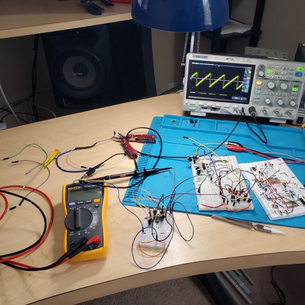
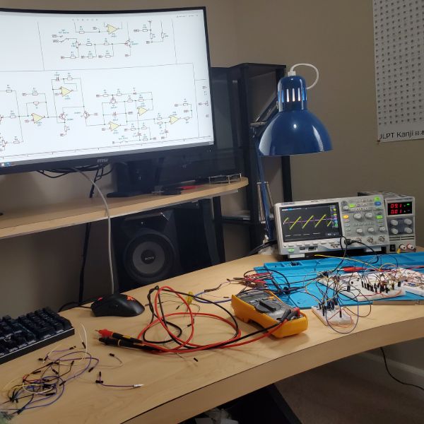
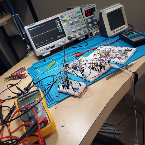
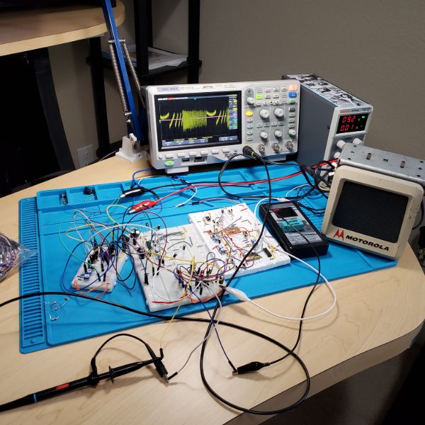
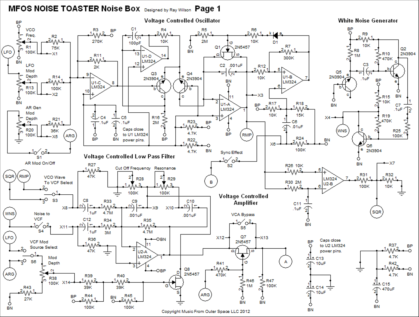
Summary: My goal for this two week block was to build out the synth on a breadboard (again) following the KiCAD schematic, to verify that there were no errors or missed connections in the Schematic, that way when I order a board based on that Schematic, the PCB actually works. The Synth is complex and has multiple submodules, which makes it very challenging to build and debug on a breadboard. I lost some productive time in week two because I had to fly to Phoenix over the weekend for a work trip, and then had to play catchup with the remainder of the week.
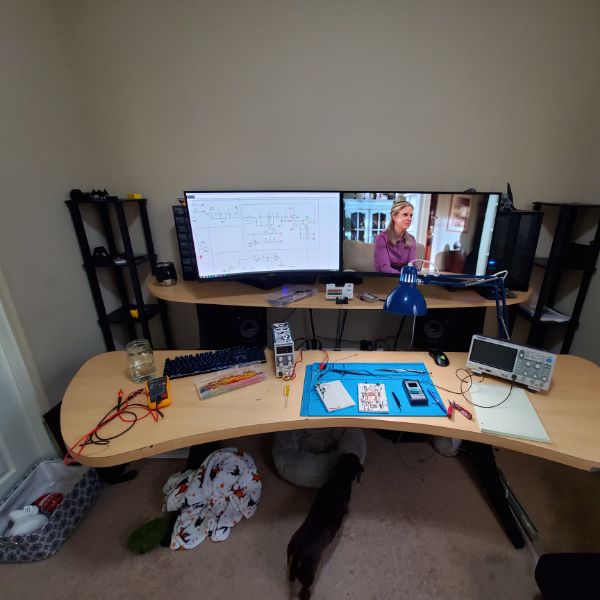
The Synth makes all the right noises, but it’s not ready to be recorded yet. I am still making sure everything functions exactly as intended, ESPECIALLY making sure I can tap a line out for the output signal and record it via Audacity by plugging an aux from the breadboard into my computer.
I was able to build out the core of the Synth and verify it works according to the schematic, as well as correct some errors in the Schematic, and I was able to adjust some of the components and the layout of the design to better suit my needs. I moved a few resistors and capacitors around to get better response from the amplifier, and a better frequency range out of the VCO set voltage. I also adjusted the input stage of the ramp’s op-amp threshold set to produce a sharper ramp. It was rewarding modifying the circuit to my needs and seeing good results from following my design intuition.
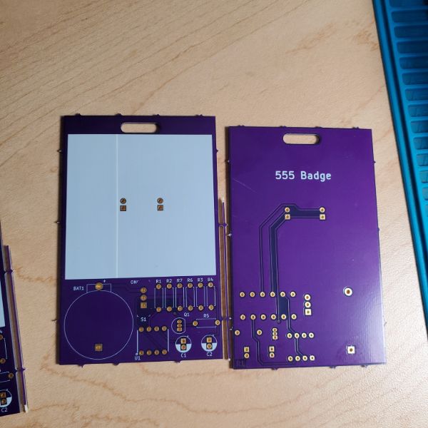
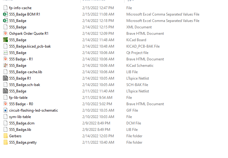
The PCBs from the 555_Badge project that I used as a KiCAD tutorial arrived on the last day of Sprint D, so assembling them will be for the E block. I’m also going to lose some time on E because I have to go out into the field for the first week of E. We’re also planning a road trip for the end of March, so I’m out and about a lot lately.
I experimented with the Fritzing Breadboard Layout software, so I could come up with a plan on building out the Breadboard for the Synth digitally before physically, but the program was just too cumbersome. It seems like it’s only really good for showing how to wire sensors and such in isolation, and not good for modeling more complex circuits.
I also followed the template from the 555 Badge’s Bill of Materials generation video, and decided to start sketching out the new Mega Lights. I’m replacing the old RGB strips on my desk with some digitally addressable, fancier ones. I’m also planning on doing the installation much more carefully so the quality of work more closely matches the effort I put into the desk. Once they’re installed, I’ll have something to manipulate via MQTT and the smart home/cyborg nest project can start expanding again after the bootcamp. The only problem is that the BOM is like $300 because I need 8m of LEDs.
I’m finding that the Synth project is actually more complex than the Power Supply, but part of the reason I’m doing it first is so that I can cut my teeth and develop finer mastery over the full design process and toolchain. That way when it’s time to work on the Power Supply, I won’t have to learn any new skills. Just figure out how the circuit works, simulate it, build a schematic, build it on a breadboard, verify its performance, route the board, order the board, build the board, and design and print an enclosure for it. The Synth has also been giving me trouble since 2020, so I’m really itching to overcome the challenge it’s presented me for so long. I want to get it into a box and give it some slick knobs and then throw it in my closet forever lol.
Dolphin
Timeline
January
A
3D Printer
B
3D Printer
February
C
Power Supply
D
Power Supply
March
E
Power Supply
F
Interview Questions
April
G
Interview Questions
H
Intel/Quartus
May
I
Tutorial Sites
J
Tutorial Sites
June
K
FPGA Projects
L
FPGA Projects
Interview Questions
4 weeks
Intel FPGA
2 weeks
FPGA Projects
4 weeks
Power Supply
6 weeks
3D Printer
4 weeks
C/C++/Python
Verilog
Art of Electronics
Next Steps
Synth Breadboard Layout
Set up Fritzing
Fritzing is Open Source, but they ask for a donation and don’t take no for an answer
This means you have to download it on github and build it yourself
But to build it you need Qt installed
What the hell is Qt?
Seems to be a C++ based GUI/App development platform. They have an enterprise license but are still open source. Their stuff looks pretty slick
Finished installing Qt. Having trouble building the App according to the github’s instructions.
I think I don’t have g++?
Picking this up tomorrow
https://www.sefidian.com/2020/05/09/installing-g-c-compiler-on-windows/
https://github.com/fritzing/fritzing-app/wiki/1.2-Windows-notes
Had some free time since work was slow. Got super mad trying to figure out how to build this thing. I stopped caring and just paid the $8 euros or whatever for the windows installer.
They totally got me lol
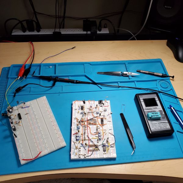
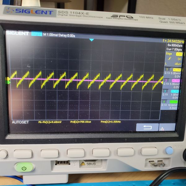
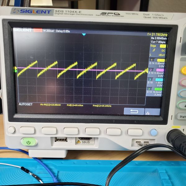
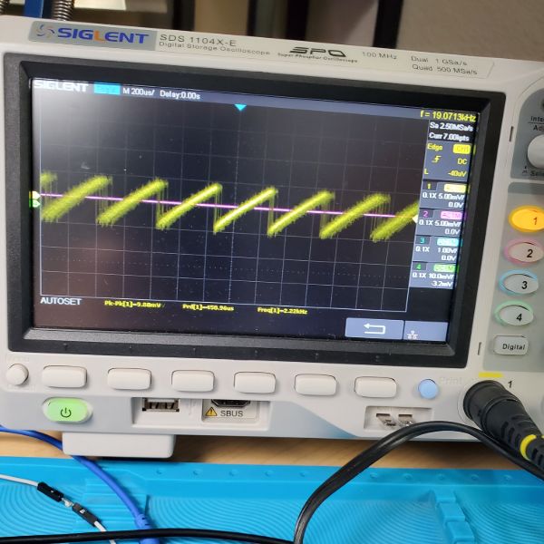
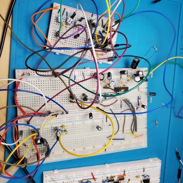
After building out the entire VCO and AA circuits on the main breadboard, and neither of them working, I modified the AA until it worked and then rebuilt the VCO circuit on a different breadboard entirely.
I’m using jumpers now because the solid core cables are just too much hassle to deal with and I’d rather deal with signal interference than have to spend 2 hours every day hurting my fingers against a stiff breadboard slot clip
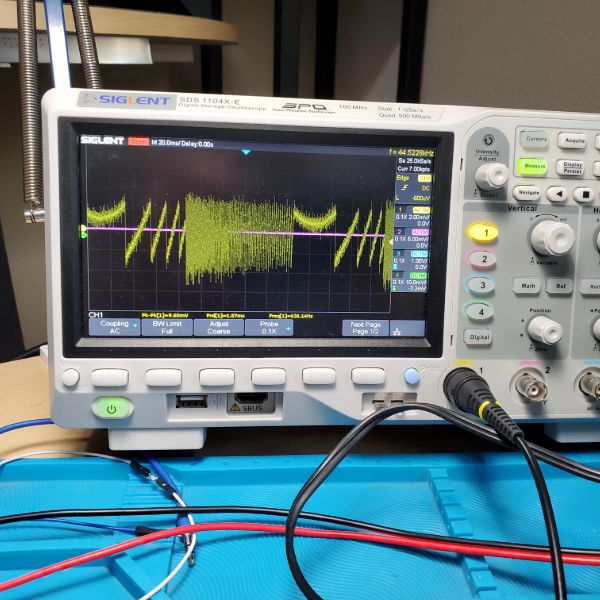
After I got the AA working, an interesting thing happened. When adjusting the pot with a screwdriver that controls the input signal’s volume, the metal of the screwdriver made contact with the body of the pot and then the screwdriver acted as an antenna, and managed to pick up some rock music.
I’ve read before that you can accidentally made an AM radio playing with op-amps, so I’m guessing I did that, or something similar. The noise was much louder when I was also touching the antenna with my finger. I’m not sure why. It’s pretty cool though. Easily avoided.
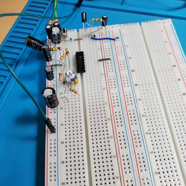
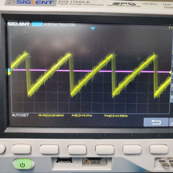
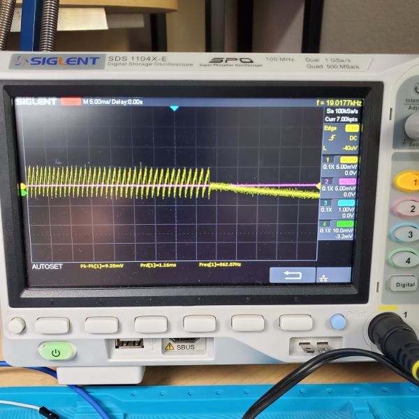
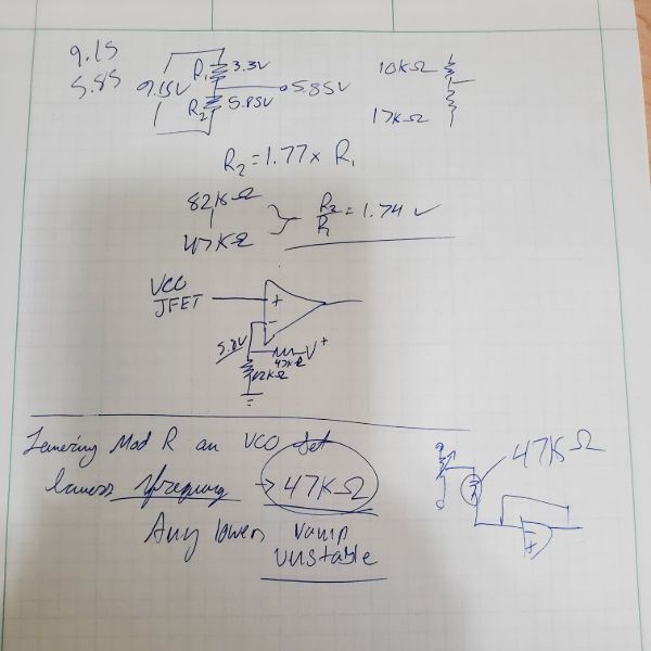
After rebuilding the VCO on the smaller breadboard I was able to get the ramp wave out of it, but I noticed that the frequency was way too high, even at the bottom of the range. I figured I might be able to adjust the feedback op-amps set voltage, so I used a pot and swung it around 5.8V. This caused some clipping on the top of the ramp wave, so I tuned both the input voltage and the feedback set voltage until I could get a properly sharp ramp wave across the full range
After I got that, I took some measurements, and came up with some resistor divider values that will allow that to hold without a pot, and that worked fine.
As for the frequency of the ramp wave being way too high, I figured that it could be adjusted by changing the flat mod depth resistor after the input voltage pot, and I was right.
By increasing that resistor, I lowered the current heading towards the op-amp input, and that managed to increase the frequency. So I started lowering it until it got to a point where the ramp wave could collapse. The most stable value I found was 47k, and that allows me to produce sub-kHz frequencies.
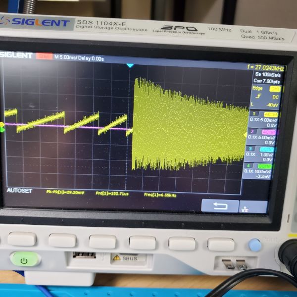
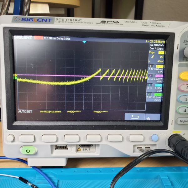
After I was satisfied with the voltage adjust/frequency adjust for the VCO, I started tying in the LFO and AREG signals, which worked as intended. Just fine actually. When I first built this thing, each knob on each pot was a mystery, but now I have a deeper understanding of what turning that knob is actually doing to specific voltages and currents inside the circuit, and so the whole thing is a lot more intuitive.
There’s still some interference and feedback and static. I’m hoping these go away once I get the thing onto a PCB and there aren’t as many wires running over eachother.
I don’t have as many pictures for this breadboard layout yet, but I will probably take a lot of the waveforms at the end once it’s working
All that’s left at this point is building the Square wave section of the VCO, and then the VCF, which is technically the biggest subcircuit.
Following what I’ve learned from the VCO, I’m going to build the VCF on a separate breadboard as well. I’m hoping this goes as smoothly as the VCO.
Once I have everything Functional on a small network of deeply interconnected breadboards, I plan on extracting each pot from its location, placing it onto a blank breadboard, and using that as a mock front panel before routing and ordering the boards.
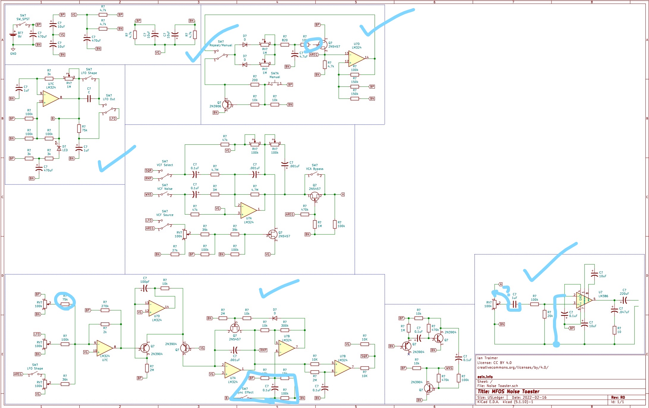
It’s also important that I compile all the slight changes to the circuit, as well as the slight errors I’ve found in the schematic. Many resistor values have been changed in the breadboard prototype simply because I don’t have those values and am not going to waste 4 resistors building them. I’ve found some missed connections on the KiCAD schematic as well. Which is good, because that means building the breadboard synth for the THIRD TIME wasn’t a waste of time.
I’m hoping to have this whole thing buttoned up inside a nice box in the next 2-3 months and then I can finally put this Synth to rest. The first time I tried to build it in Nov 2020, I had no idea what I was looking at. Sometimes I wish it didn’t take this long or I never tried lol. But, perseverance and time make the magic happen
Synth PCB Layout
Building Schematic in KiCAD
Spent today’s lab session building out the LFO and AREG on breadboard, both work fine.
Next is the VCO, which I’ll set up with just the voltage control first to verify, now that I know how it’s supposed to work. Once I’ve confirmed that it works, I’ll tap in the LFO and AREG signals and test the combination
Found some bugs in the KiCAD Schematic as well
I should come up with a functionality checklist for the breadboard Synth
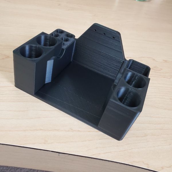
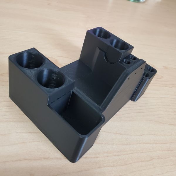
One of the most important features that I want to ensure works on the finished product is the line out feature. I need to make sure the finished circuit can actually tap out into an aux jack and go into a computer and get recorded via Audacity. That means the synth can actually connect to a digital system and get sampled, which is important to me.
I’m hoping to be able to distribute a few copies of the finished synth once the whole thing is completed. I’m guessing that, if I want to make that the distribution present for christmastime this year, I’m going to have to do 2-3 revisions of the PCB to add features and package it properly.
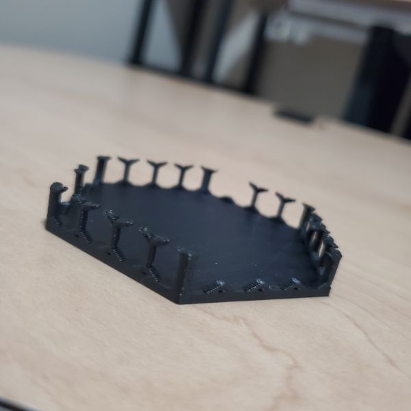
One thing I’m not quite prepared for is the casing. It’s easy enough to make a housing for a PCB, but since I have to make a front panel for the whole thing, I’m not sure if 3D Printing will be appropriate. The dimensions will be fine and the pots can be rigidly mounted, but I don’t know how to mask a UI onto the front panel of a 3D printed plane like that. I’m sure there are answers online
Further, for power supply, I started thinking about using a rechargable LiPo cell. But I’m pretty sure those are almost all 4.5V or below, which means I would have to use a Boost Converter which might affect audio quality with spiking in the power supply. On top of that, the current draw would be higher than normal. I’m guessing the synth is pretty low power. I think it only draws 15-20mA when it’s working, but that speaks nothing of the audio amplification, which could go up to a 1/4W.
.25W / 9V = 27 mA
20 mA + 27mA = 47 mA ~= 50mA
9.6V LiPo cell 2000mAh: 40 hours of synth time
That’s wrong. A quick sim shows the peak current going through the speaker will be 780mA 2pk. So the amplitude is about 390. The RMS current is 0.7071*390=275mA
275+20 = 300mA
300mA on a 9.6V LiPo cell 2000mAh: 6 hours
I could design it with both a barrel jack for 9V AND a 9V Battery slot, but I don’t think that’s worthwhile just yet. It’s probably cheaper than adding a rechargable cell to each instance, so I may get there in the future, but for now I’m going to just assume it’s plugged into the wall.
I’m thinking it might be worthwhile to make a mockup of the front panel now, before I order a PCB, so that I can ensure that everything will actually work as intended. It’s one thing to experience a bunch of boardboard switches and pots as functional. It’s another to make a tangible UI to the project that can be adjusted more intuitively.
Design a sheet of PLA with holes in it for the pots
Design some handles for the tiny pots? or just use screwdrivers for this
Design holes for the switches as well
Mask it with a sheet of paper for labeling, or use the label maker
Mount everything into the PLA Panel, solder wires that can connect back to the breadboard
Follow the advice of the book on signal interference
I could also just get a second breadboard and jump everything over to the original breadboard, and have only UI front panel components on the second breadboard. That would be just as good with significantly less intermediate design work. It won’t change the fact I’ll have to design a front panel sooner or later though.
For the breadboard as I left it, I have the LFO and the AREG working. Next is to make an unmodulated VCO circuit, which will take a while. Then the AA, to verify that the VCO can produce an audible waveform. From there, I’ll have a basic functionality that I can then tie in the AREG and LFO to, to ensure that all the features work
Once I have completed the checklist via the breadboard, then I can move onto designing a front panel mockup. Once the breadboard synth and the front panel mockup are satisfactory, I can move onto designing the PCB in earnest, with the confidence that I have a fully functional prototype. That will be the more fun part for sure.
I’ve been thinking a lot lately about how the synth is probably a more complex project than the power supply I’m using it to prepare for. But that’s fine. This is worthwhile engineering work for me. I’m going to beat this Synth and not let it frustrate and overwhelm me. And then I’ll get to share that victory with others
Notes on Schematic Changes from Breadboard Tweaking
Resistor on Exp.Wave output on LFO changed from 75k to 20k
Changed Flat Mod Resistor on Voltage input to VCO (VCO Freq) from 75k to 47k
Connected JFET properly on AREG (not connected on schematic)
Skipped Sync Effect on LFO. Still needs to be tested. Currently using a simple voltage divider at a tuned voltage of 5.85V, with a source voltage of 9.15V
Put Coupling Capacitor on AA ahead of the pot
On AA, LM386 Pin 2 and 4 are not connected to ground in schematic
Synth Schematic Performance Checklist
PSU
Maintains a virtual ground of 50% dV
AREG
Produces Attack-Release Envelope
Repeat/Manual function
LFO
Adjustable Low Frequency
Produces Square Wave
Produces Smooth Wave
Produces Spike Wave
All output waves selectable to LFO node
VCO
Voltage Controlled Frequency of Ramp Wave
Ramp Wave converts to Square Wave
Modulation by AREG
Modulation by LFO
Sync Effect Functional
VCA
VCA amplifies output signal according to AREG signal
VCA Bypass switch functional
WNS
White Noise is audible when fed directly to output
White noise has an audible effect when mixed in
AA
AA Can properly drive the speaker
AA has meaningful volume adjust
AA can run for extended duration without overheating or damaging anything
AA can effectively line-out to an external speaker
AA can effectively line-out to an external computer and be sampled via audacity without incident
Power Supply Design Videos
Power Supply LTSpice Simulation
Power Supply PCB Layout
Power Supply BOM
Synth BOM
Fritzing Tutorial
https://youtu.be/-saXw1EipX0
Hold Shift while placing wires to get them to snap to axes
double click or click and drag wires at any point to create a bend
Check View > Align to Grid. That feature is cringe and makes it hard to line up components
You can copy paste component selections
You can move selected components with the Arrow Keys
Import new Models
FZPZ file type
https://arduinomodules.info/download/ky-016-rgb-full-color-led-module-zip-file/
Click and Hold on a Node to highlight all connected nodes in yellow.
Good Sanity Check Tool.
Also, just started imagining electrons flowing from ground for the first time…
When you make changes to the breadboard, you automatically make changes to the schematic and the pcb as well.
I’m guessing once you finish one all pretty it’s in your best interest to make sure the other ones are pretty as well…
https://github.com/tardate/LittleArduinoProjects
After some basic construction, I’ve decided that Fritzing isn’t going to be as useful as I was hoping towards laying out a model for the Synth. There’s too much part graphic overlap to get a clear picture. I’m just going to build the breadboard based on the Schematic
Power Supply Design Project
C1
LTSpice Tutorials, LTSpice Modeling Projects
C2
KiCAD Tutorials, KiCAD Modeling Projects, LTSpice Modeling Projects
D1
Finish KiCAD Tutorials, Order 555 Badge PCB, Watch Power Supply Design Series, Model along in LTSpice, Peripheral Research. Lay out board for Synth
D2
Watch Power Supply Design Series, Finish LTSpice Model, Build KiCAD Schematic, Lay out Board, Order PCB, Peripheral Research. Lay out board for Synth, Order PCB
E1
Waiting for parts and PCBs to ship. Interview Questions.
E2
Waiting for parts and PCBs to ship. Interview Questions.
F1
Assembling and Soldering PCBs. Designing and Printing Housings in FreeCAD. Interview Questions
F2
Assembling and Soldering PCBs. Designing and Printing Housings in FreeCAD, polishing projects, documentation. Interview Questions
Resources List
Monty Choy Hardware Interview Questions
1
Digital Design HQ Discord #Resource Dump
2
EEVBlog Power Supply Design Series
3
Intel FPGA Technical Trainings
3
Digikey intro to RTOS
4
Digikey intro to FPGA
4
Digikey intro to KiCad
D
EP 7 – Board Layout
https://youtu.be/jaQPr7PgImk?list=PL3bNyZYHcRSUhUXUt51W6nKvxx2ORvUQB
Time to lay out the board. Want to finish this and order by Wednesday at the latest so I can start moving onto the Power Supply Design Videos
Once the board is laid out and ordered, I also need to arrange a BOM and order from Digikey for that. I already have all the components necessary to populate this board, but I want to follow thr process through completion including component stocking and I consider that worth the $20 or whatever it’s going to cost to buy a 555 and some basic components.
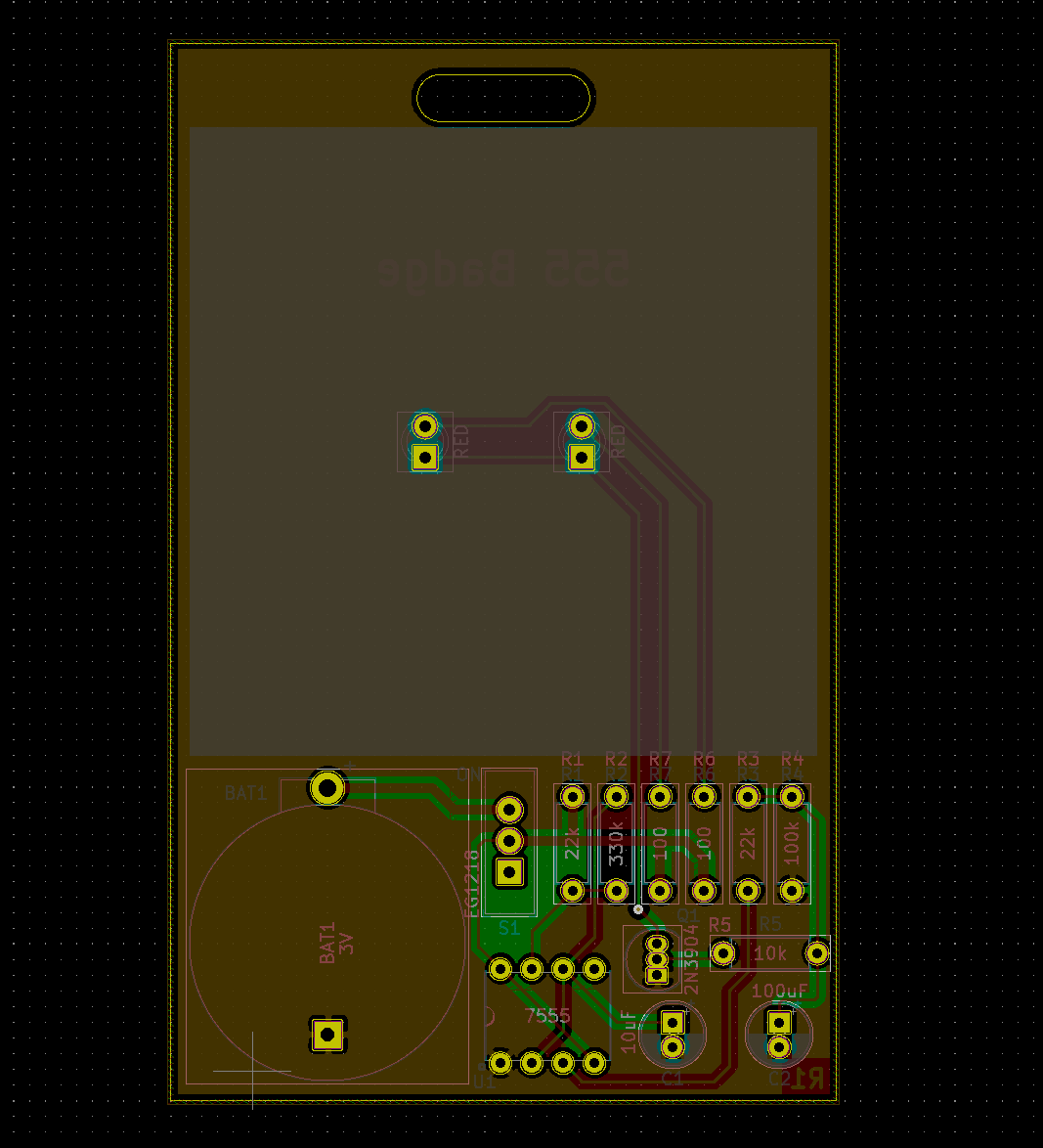
It’s a good idea to periodically run the DRC (ladybug icon) while laying out the board. Run it before you start as well.
Found an issue with the first DRC run. The pads of the transistor Q1 were too close together and violated the 10 mils clearance demanded in the global design rules.
I wanted to get rid of this, so I checked the Osh Park KiCAD design rules page online and it says the minimum clearance is 6 mils, so I lowered it from 10 to 6 and reran the DRC and now it’s passing.
Routing
Select Route tool
MAKE SURE YOU’RE TRACING ON THE CORRECT COPPER LAYER
Click a pad
Start moving mouse to lay out a trace
Click to lay down a bend midway
Mouse over the terminal pad
Double click to finish the trace
press escape to cancel the trace
No real correct order to make the traces but, some general rules
Make Power Traces first
Then Make close connections
Then work on complicated routing
Power Traces need to be thicker than signal traces because they’re thicker
Trace Width Calculation
If you know how much current a power trace is expected to conduct, then you should use a trace width calculator to determine the appropriate width of the trace, based on the specs of your board
Advanced Circuits’ Trace Width Calculator
https://www.4pcb.com/trace-width-calculator.html
From the LTSpice Simulation, I know the peak current draw of the battery, and the peak current draw of the LEDs.
The Video shows a 20 mA spike, but my simulation, which is identical as far as I can tell, only shows 12 mA. Using the 20mA number for padding.
When doing Trace Width Calculation, pay attention to the thickness of the copper in the calculation. Most boards are 1oz Copper unless you want to pay extra for 2oz Copper.
The calculator will yield two sets of results for traces on internal layers of copper, and for those on the outside. It looks like the layers on the inside need to be thicker. I’m not sure why
The minimum trace width is .05 mil. Since the default trace width I’m working with on this board is 10 mil, there’s nothing to worry about. Trace width doesn’t become a serious concern at 10 mil until a few hundred milliamps.
Setting up multiple Track Widths
For complicated projects, you can create Net Classes with different parameters, hole sizes, clearances, track widths etc. And then assign those Net Classes to different nodes/nets within the PCB.
This way they already know and are assigned their track widths
Otherwise, you can basically set up a hotbar of a few different track styles and swap between them at your discretion
Just open Design Rules, go to Tracks & Vias, and add a Track Width
From here, you can use the dropdown next to the grid size in the main window to select between your pre-made track widths:
While tracing, I realized I missed a connection on the Schematic, that I didn’t miss on the LTSpice Simulation. Pin 7 of the 555 connects to the voltage divider. I was worried this would create a big fuss, but it went over pretty well. I reopened the schematic, updated the page settings for an R1. Made the connection, ran the ERC. Then exported the Netlist as R1. Then opened the PCBNEW tool again and loaded the Netlist.
That action cannot be undone, I was worried it would dump a fresh set of every component onto the PCB, but it didn’t. It just updated the pin/net connections on everything where it stands using the new netlist information
Older Board Manufacturers could only pick and place, and mill and route on 90 or 45 degree angles, which is why that’s reflected in design software.
Above 1GHz, there will be signal reflection issues if the trace curves at a 90 degree angle.
Avoid Acute intersections of copper as well
The corrosive chemicals used to etch the copper can get caught in acute angles and corrode the board after its finished being manufactured.
This is called an Acid Trap
Vias
While routing a trace, press V
Drop the via, and you’ll keep tracing on the underside layer
Zone Filling / Copper Pour
A great way to connect all the grounds, and to save the manufacturer time and money, is to fill the board space with copper and just say it’s connected to ground.
Draw a box just outside the perimeter of the board. Select the copper layer and the node it will connect to
It seems like the Zone Fill tool will ignore isolated sections within the PCB that don’t have a ground to connect to. Not everything will be filled, and that seems to be okay.
Once the board layout is complete, run the DRC again to check for any issues.
This is your new best friend
Silkscreen
Feel free to add text notes onto your PCB using Silk screen
Remember the KiCAD visualization lets you see straight through layers, so if you want some text on the backside of the board, you have to mirror it in options so it appears properly after fab
If you want to add text in copper, but you’ve already added the fill zones, just press B at any time to recalculate the fill zones
EP 8 – Generate Gebers and Order Boards
https://youtu.be/ENmDnoKs2hM?list=PL3bNyZYHcRSUhUXUt51W6nKvxx2ORvUQB
Finally
Gerber is the name of a corp that made a vector photo file format. Those are similar to PCB manufactureres, so they took it.
One gerber file for each layer of your board, incl. non copper layers
Go to the board house website and find the page for generating gerber files.
Just like the board design rules setup and net classes, you have to check and uncheck whatever boxes they ask you for.
Generate the gerbers for the requested layers and the drill file. Save your PCB and close out.
Next is to open GerbView and verify that the gerber files exported correctly and they look all good before sending out to fab
The sequence in which you open the Gerbers seems to matter, but I’m pretty sure you can just rearrange the layers after loading anyway.
Drill Hits
Edge Cuts
F Silk
F Mask
F Copper
B Silk
B Mask
B Copper
The Solder Mask layer shows what areas will be EXCLUDED from the solder mask. Specifically, creating the annular ring around your drill holes:
Verify that the top side looks good, then check the bottom side
EP 9 – Generate BOM and Order Parts
https://youtu.be/I7GUiGoD1w8?list=PL3bNyZYHcRSUhUXUt51W6nKvxx2ORvUQB
BOM is what separates the pros. It’s really good design documentation and makes it 1000x easier to replicate. Take your time on it every time.
There are a lot of BOM Generating Plugins for KiCAD. Maybe take a look around and see what you like
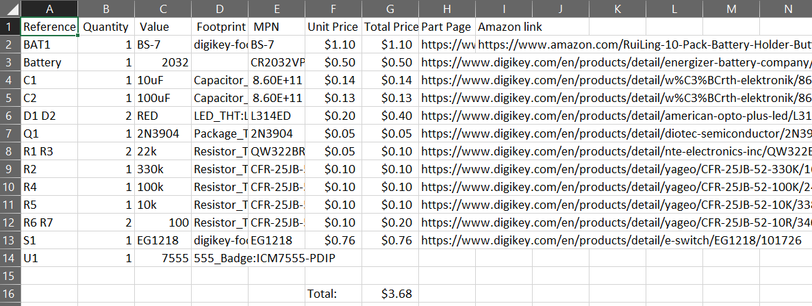
Open the schematic and Tools > Generate Bill of Materials
Use bom2grouped_csv
Finished Bill of Materials should look something like this
Some notes
I already have everything here except for the battery, the battery holder, and the switch
I’m having trouble finding the battery holder somewhere that isn’t digikey.
I don’t have the time at the moment to check the amazon substitutes against what I was expecting
I might have to come up with a bigger cart to justify making a purchase on digikey
I already have the EG1218 switches, or at least a dimensional equivalent. They’re discontinued though.
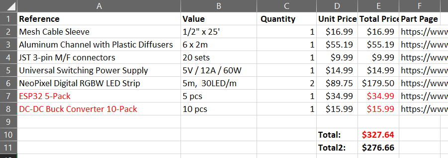
This might be a good time to purchase some sample LED strips for the new mega lights, and maybe some other stuff too.
It’s like going to the grocery store, you just pick more stuff up that you weren’t looking for since you’re already there.
After doing some research on the LED Strips, so I could fit them into a Digikey cart, I decided that I would need 5m strips, and digikey only has the ones I’m looking for in 1m segments. So I’m skipping the digikey order entirely and just finding an Amazon Alternative
https://www.amazon.com/RuiLing-10-Pack-Battery-Holder-Button/dp/B07VRYKG9G/ref=sr_1_15?crid=293W0WIEXWK5B&keywords=battery+holder+2032&qid=1644951772&sprefix=battery+holder+2032%2Caps%2C104&sr=8-15
After some digging, I found a CR2032 coin cell holder on amazon that seems to have the same general profile as the BS-7 I was looking for. The description said the leads are 20mm apart, so I opened KiCAD and confirmed that the drill hits for the two terminals of the BS-7 are 20mm apart. So that one is good to order. The only issue is, I’m going to get like, 10 of them in the mail now. So I’m also going to order a back of CR2032 cells, since I’m going to have to use at least three batteries to assemble all the boards.
It will also be nice to have some extra batteries, since buying them is super expensive at the store when you only need one or two
Placed the Order for the batteries and battery holders.
I’m pretty sure I have enough 555s for the three badges. Double checking that and 2N3904
I’ve got 8 555’s on hand.
I also tested the breadboard circuit with a 2N2222 and the performance seems identical, despite LTSpice claiming there was a notable difference in LED current.
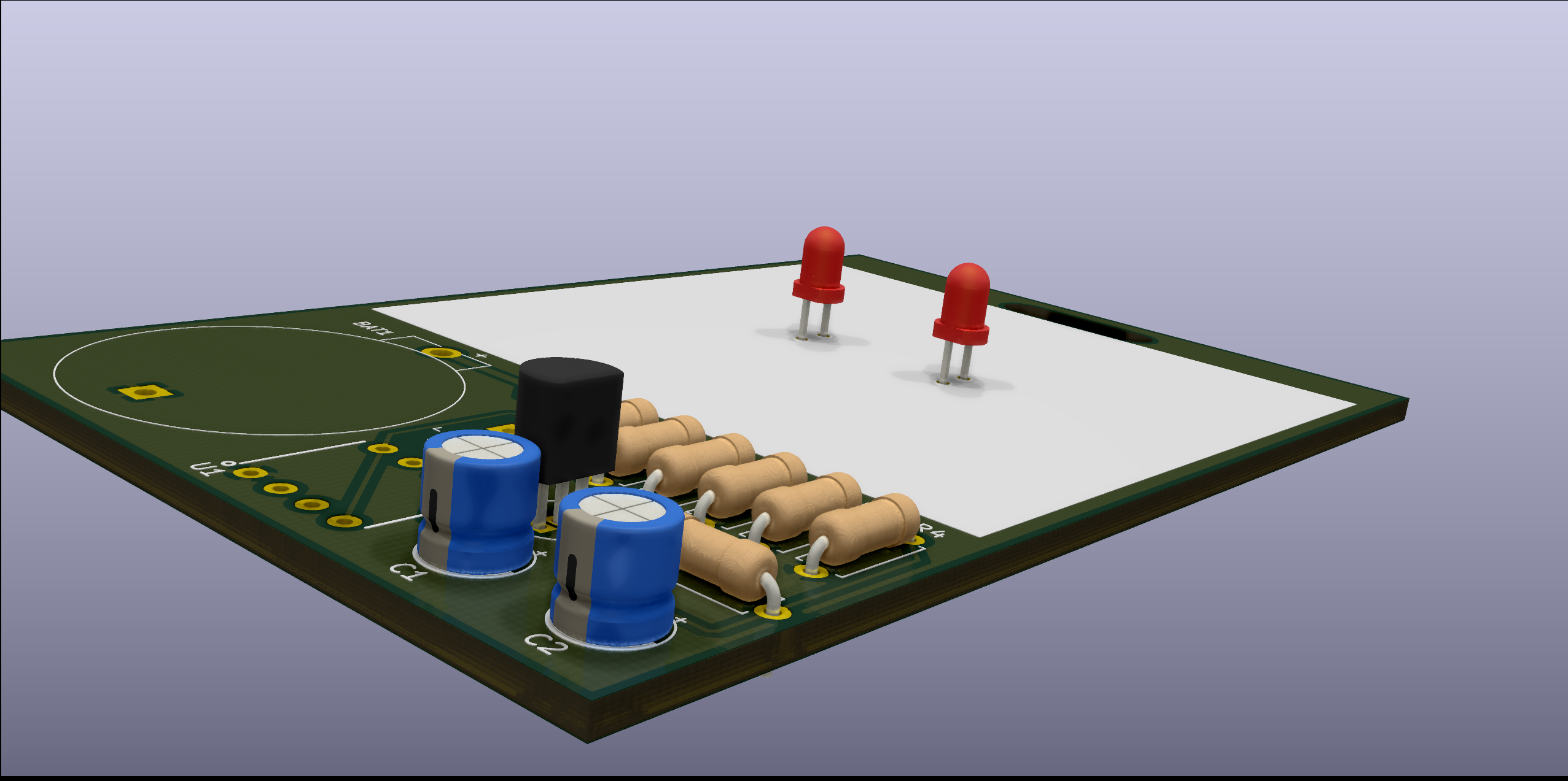
EP 10 – Solder Components to the PCB
https://youtu.be/Zkn_Au5aeLA?list=PL3bNyZYHcRSUhUXUt51W6nKvxx2ORvUQB
2/14/2022 – PCBs Ordered
4
FesZ intro to LTSpice
4
Tutorial Sites
Asicworld
ZipCPU
Nandland
cplusplus
Practice Problems for Hardware Engineers.pdf
FPGA4Fun
Nandgame
HDLBits
EDAPlayground
FPGA4Student
Bitsolver
5
Art of Electronics
5
Automate Boring Stuff with Python
6
C++ for Embedded Systems
6
3D Printing Dive
7
FreeCAD Tutorials
7
General Project Timeline
1
Watch Power Supply Design Series
2
Follow Tutorials to LTSpice
3
Follow Tutorials to KiCAD
4
Apply Tutorial Knowledge to Power Supply Design Series
5
Creating a working Simulation of the Power Supply
6
Create a presentable Schematic of the Power Supply
7
Design a PCB for the Power Supply and Place an Order at JLCPCB
8
Order Parts for the PCB
9
Design an Enclosure for the Power Supply and Print it
10
Assemble and Personalize the completed Power Supply
Other Ideas
Put Megadesk in Minecraft
MQTT home server to minecraft
Weather station for Breadnet
Fried Cricket Chips
Chip warming bowl for chips and salsa
VR Safety Training Videos
Water Cooled Bluetooth Plasma Speaker
Give the Synth out for Xmas
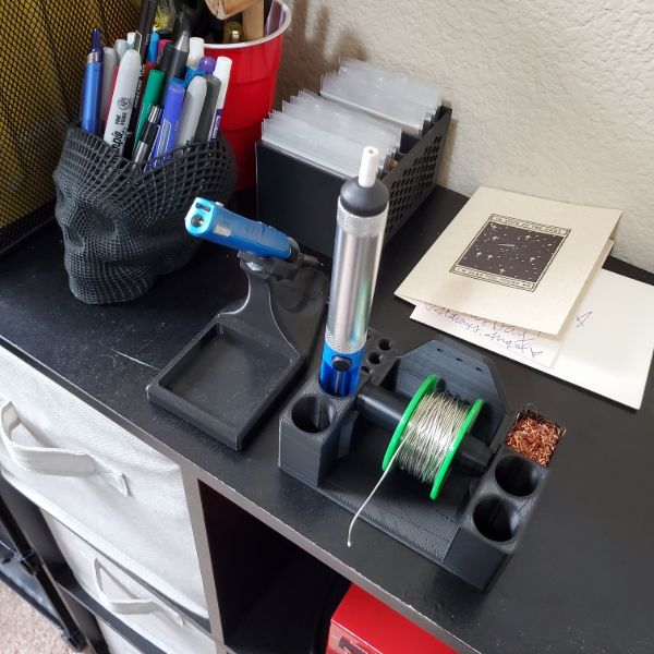
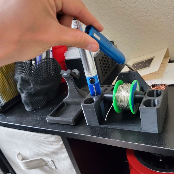
Desk mounted soldering station
Turner Cube mount spinner
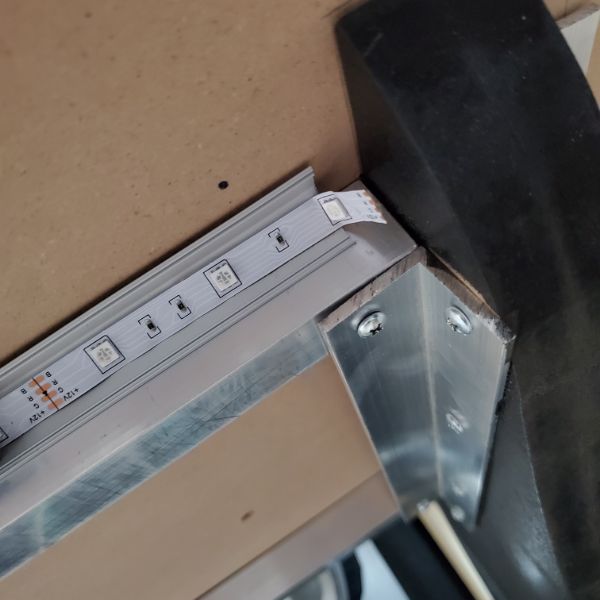
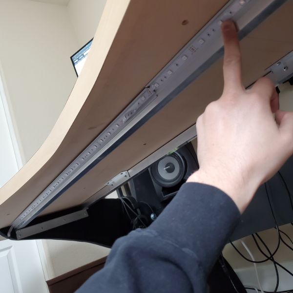
LED Strip Research / Breadnet Project
Lab stuff, I have been kind of avoidant and dreading diving into the power supply. I feel like I don’t have enough time to get through the whole power supply series in just 2 weeks. Along with the Synth that I added on. If the Synth gives me as much trouble in layout as it did in Spice then I’m going to have an issue.
And if the Power Supply gives me as much trouble in either Spice or Layout as the Synth did in Spice, then I’m going to have another big issue. So I’m just generally not looking forward to getting started very much, so I spent a day researching some other stuff. Printer Upgrades, Desk Upgrades, Anti-Static for my chair, etc.
BOM
Parts will cost around $300
These aluminum channels are super expensive, so it’s in my best interest to go find the spares, if I didn’t throw them away.
But honestly, they looked super shoddy being constructed out of 1m segments
I might just drop the extra cash to get them 2m
Ideally, I would just buy 4 x 2m LED Strips, but that doesn’t seem to be an option
Even if I bought 7m at $18/m, that’s still $126, and then they look super shoddy and patchworked together. On top of multiple 10mm deadzones from adapters connecting together.
It looks like on two separate cases I’m spending an extra $50 just to make it look prettier
Comparison Video
https://youtu.be/QnvircC22hU
Power Consumption
Model
Voltage
Idle 0 LED
Single Channel per LED
RGB Channel Per LED
Single Channel, ALL 150 LED
RGB Channel, ALL 150 LED
PURE WHITE, ALL 150
SK6812
5
.83W
.05W
.148W
7.63W
14.4W
10W
Looking at the SK6812, as they are the only strip with a white pixel
Adafruit RGB Strip Product List
https://www.adafruit.com/category/183
Checking the data sheet, it looks like they have a max refresh rate of 30Hz
http://www.led-color.com/upload/201809/SK6812%20RGB%20LED%20Chip%205050%20Datasheet.pdf
Purchase Links
https://www.digikey.com/en/products/detail/adafruit-industries-llc/2828/5959337
https://www.adafruit.com/product/2824?length=1
Adafruit is the only reliable vendor for the SK6812 strips.
I’m looking at the black flex PCB with the minimal silicone sleeve. The 30/m strips run about $18/m. I am not sure how many meters I need though
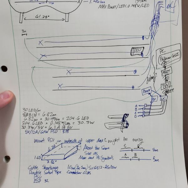
Desk is divided into Upper Desk and Lower Desk
Both Desks have two aluminum rails, and LED Strips go on the out-facing sides for both rails for both desks, so four strips in total
Upper Desk Rail Length: 1.95m
Lower Desk Rail Length: 1.46m
Total Length to Cover: 6.82m
SK6812-RGBW’s are only in stock in 1m and 5m variants. I’ll need 2x5m
Project Steps
This whole thing should probably be a part of a larger project of setting up the Smart Home in earnest.
Which would involve me learning more optimal MQTT, Learning the ins and outs of Node-RED and HASS. Connecting my 3D Printer to the Breadnet
Some Security Oriented work
And then setting up a logging database like a weather station that can be repurposed into crickets in the future
Also includes ESP32 Over-The-Air Updates
Also Includes the Python GUI project for the mega lights
So
MQTT Dive
Node-RED Dive
HASS Dive
Weather Station
Mega Lights
Mega Lights GUI
ESP32 OTA Updates
OctoPrint
Network Security
ESP32 Low Power Deployment
Sounds like about 1 full month’s worth of work. So I’ll save that for later, after I’ve finished the 6 month to FPGA bootcamp
Wiring
I’m thinking I’ll have all the wires on the right hand side of the desk.
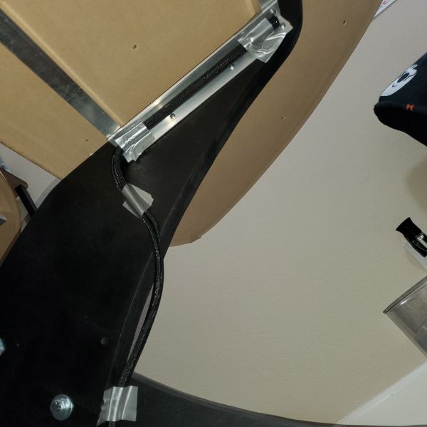
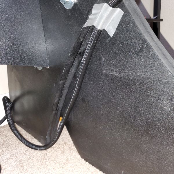
From the front-lower strip, I’ll run a mesh cable sleeve like the one I used on the 3D printer along the underside, collecting the back-lower strip, and then running down the underside of the inner leg.
For the upper strips, I’ll also have the cables connect on the right hand side, going from front to back
From there, I’ll have the lower desk mesh sleeve run back up and meet up with the upper desk sleeve, and connect them using a Y-adapter into one mesh sleeve.
Then I’ll run that Mesh Sleeve to the PSU/uC combo.
To minimize cable management, it seems like it would be best to keep the Power Lines and the Data Lines terminal in the same location, so the ESP32 and the PSU are going to have to be in the same place
Power Consumption
30 LEDs/m
6.82m
204.6 LEDs
0.148W/LED
204.6 LEDs x 0.148 W/LED = 30.3W
30.3W @ 5V = 6.1A
Conclusion: Get a 5V/12A PSU
Mounting
I’m thinking about mounting the power supply on the underside of the upper desk on the right hand side, but I’m not sure that’s the smartest approach.
If I’m using a ESP32, The input voltage should be 3.3V-3.6V, but it has a regulator to handle 5V, or up to 6.5V I think.
The input output pins are NOT 5 Volt tolerant.
I think the safest approach would actually be to use the 2nd buck converter from the pack of 2 I bought for the 3D Printer, and set that to ~3.5V so the ESP has a buffer and a layer of extra regulation. Is that how power supplies work? Not sure. But I’m pretty sure that’s safer than powering the ESP32 directly from the PSU.
So if I’m putting an ESP32 and a PSU and a Buck Converter all in the same place, it wouldn’t be very convenient or elegant to mount all that on the underside of a piece of wood 4 feet off the ground.
I’m thinking the best option would actually be to run both cable mesh sleeves down to the floor and then just fashion an enclosure for the 3 Devices.
In that case, it would be simple enough to print an enclosure for everything.
Dimensions of the PSU are approximately that of Carl Jung’s Man and His Symbols
6″x4″x2″ roughly
6.26″ x 3.86″ x 1.65″ exact
Putting it in a 3D Printed Enclosure on the floor would also allow me to skip the whole Y adapted Cable Mesh Sleeve Problem as well.
This would also be a good opportunity to put my modeling and printing skills to good use in an electronics project for the first time
System Scheme
4 RGB LED Strips
Power Connection to PSU
PSU Powered From Desk Power Grid
Data Connection to ESP32
Look into OTA Uploads for ESP32?
ESP32 using NeoPixel Library
Connected to Breadnet via MQTT
MQTT hosted via RPi using HASS
ESP32 receives commands over Breadnet-MQTT via a Python Desktop GUI
PC
There are also RGB LED Strips specifically for PCs that can plug into slots on the MOBO, if that’s an angle I want to take. I kind of like it how it is now though.
If I’m going to put any more money into the PC, it’d be for a Noctua Intake/Exhaust Fan since there’s no net airflow betwen the PC and the room
https://youtu.be/8guzWUeQ3FQ
Future Upgrades
Eventually, I could replace the PSU with a 5V 12A one that I designed myself, but I’m not sure how far away that could be.
I’m also thinking about trying to sync it with keyboard presses or with audio
At minimum though, I want to create patterns that can be called at the press of a button off of the GUI
Ideally, I’d have individual control over the LEDs, which would mean the GUI would have a visual representation of each LED’s current status. From there, I could select an individual LED and set its color