
2/28/2022 – 3/13/2022
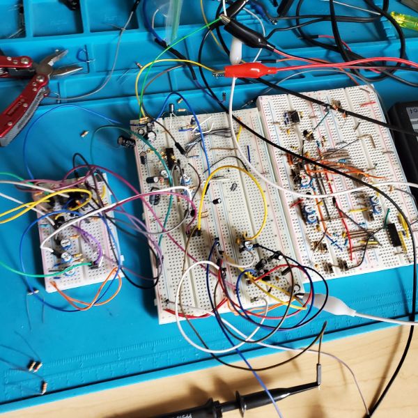
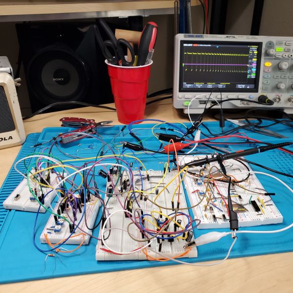
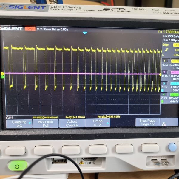
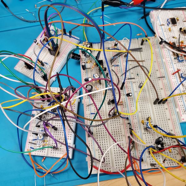
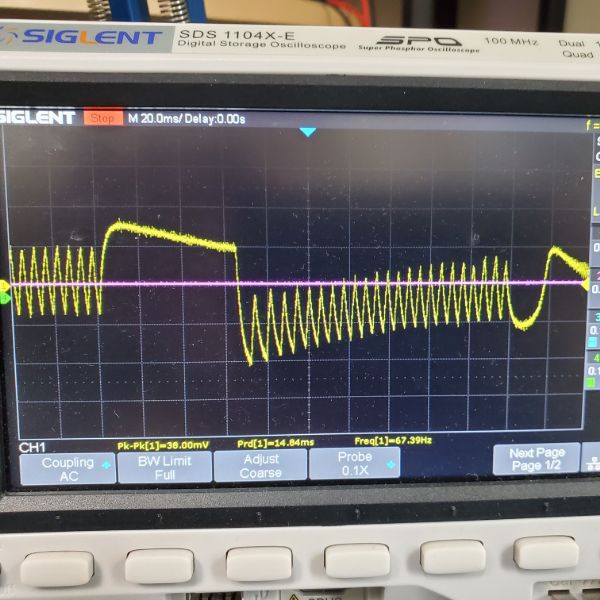
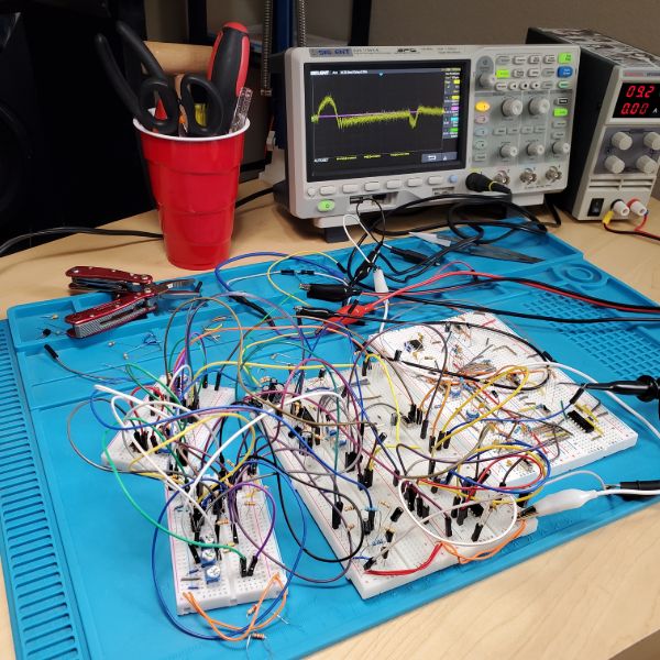
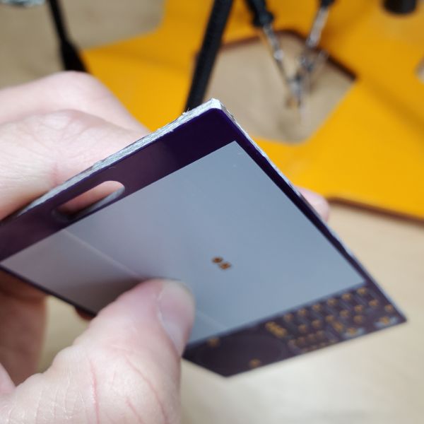
Summary: My goal for this two week block was to finish debugging the breadboard synth, make any design changes necessary, and then route and order the PCB. I got called to go onto a job site though both weeks this sprint so I lost a lot of productive lab time. My 555 Badge PCBs did show up though, and I soldered them together and figured out how to use my Dremel to trim the sides they don’t scratch people when they handle my boards. The Breadboard Synth is functioning how I expect it to now, and I can consistently recreate the Radio effect by simply disconnecting the input signal pot and placing my finger, or a screwdriver with my finger attached, to the input signal line.
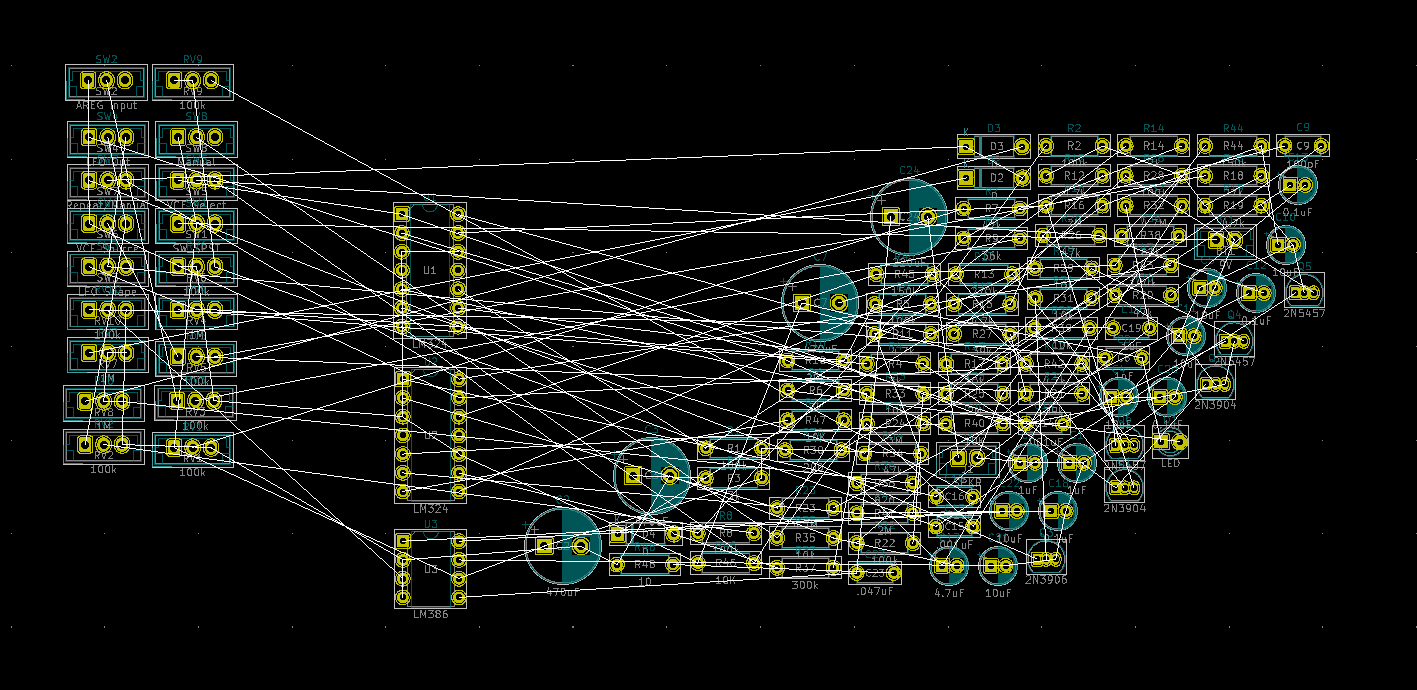
I did make some design changes to the schematic for the synth and assigned all the footprints and began routing. I’m having trouble figuring out a methodology for routing larger boards with more than 10 simple components. I’ve got two 14 pin opamps to route to and it’s becoming a confusing task to try and make a layout that doesn’t just look like an actual ratsnest/mess.
Soldering together the PC boards make me realized I don’t actually know any advanced soldering techniques. I’m pretty good at getting a good glob, but it occurred to me that it’ll probably be worth my time to spend some time soldering together some kits and figuring out how to use SMT kits, desoldering, resoldering, etc.
No 3D Prints/Modeling this week, but I did buy some new red PLA filament because I ran out of the black after a spaghetti incident.
I also spent some time planning out a friend’s office space. He needs some help installing some smart home type stuff, mounting some LED strips, building a desk, and building and lighting a display cabinet. That’s not something worth posting in further detail at the moment.
I’ll be doing field work the second week of F as well, so I anticipate there will be more interruptions for F as well. Once the synth PCBs are ordered, I’m switching gears to Monty’s Interview Questions for a bit before moving on to the Power Supply PCB. Originally, the synth was supposed to be a warmup to the PSU, but I’m guessing the PSU will be easier than the synth at this rate. Either way, I’d like to take a short break from KiCAD and its various frustrations and just check some boxes. Along with the Interview Questions, I’ll take some time to practice soldering skills and maybe model out a new soldering iron holder that can affix to my desk. While assembling the 555 Badge boards, I left the soldering iron on too long and the washer I had hot glued to a 3D printed holder warmed up and melted the hot glue, rendering the whole thing useless.
Eagle
Resources List
Monty Choy Hardware Interview Questions
1
Digital Design HQ Discord #Resource Dump
2
EEVBlog Power Supply Design Series
3
Intel FPGA Technical Trainings
3
Digikey intro to RTOS
4
Digikey intro to FPGA
4
Digikey intro to KiCad
4
FesZ intro to LTSpice
4
Tutorial Sites
Asicworld
ZipCPU
Nandland
cplusplus
Practice Problems for Hardware Engineers.pdf
FPGA4Fun
Nandgame
HDLBits
EDAPlayground
FPGA4Student
Bitsolver
5
Art of Electronics
5
Automate Boring Stuff with Python
6
C++ for Embedded Systems
6
3D Printing Dive
7
FreeCAD Tutorials
7
Timeline
January
A
3D Printer
B
3D Printer
February
C
Power Supply
D
Power Supply
March
E
Power Supply
F
Interview Questions
April
G
Interview Questions
H
Intel/Quartus
May
I
Tutorial Sites
J
Tutorial Sites
June
K
FPGA Projects
L
FPGA Projects
Interview Questions
4 weeks
Intel FPGA
2 weeks
FPGA Projects
4 weeks
Power Supply
6 weeks
3D Printer
4 weeks
C/C++/Python
Verilog
Art of Electronics
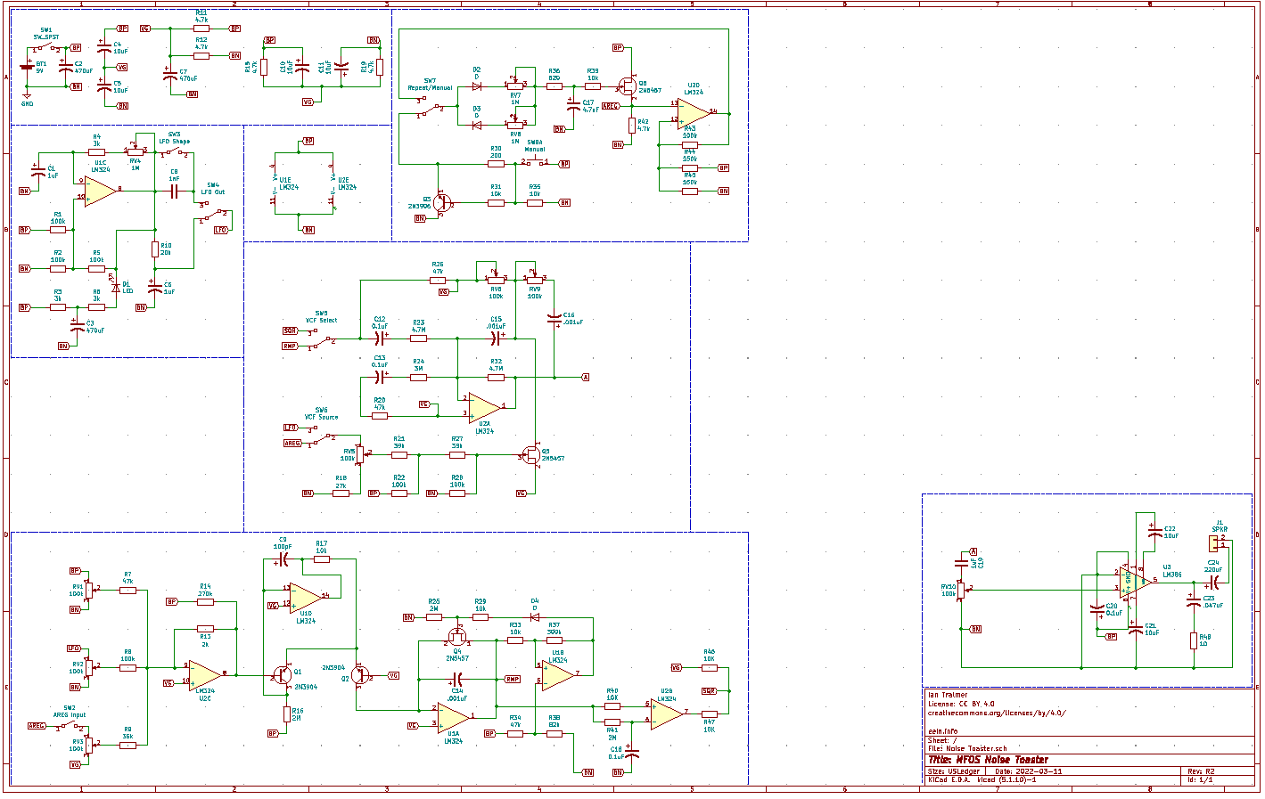
Synth R1 PCB Layout
After adjusting the schematic with the changes I found and discovered on the breadboard, it’s time to assign footprints and get moving on the board.
I’m about two weeks behind schedule now due to having to spend the last two weeks out in the field for work, and because I decided to include the Synth as another project before moving onto the power supply. Once the power supply is finished, I’m going to pore through the interview questions, and that should be sufficient to conclude the bootcamp and move on to something more specific
I do find myself wanting to push through and get through all this so I can read AoE cover to cover. I’m gonna have to do it eventually.
List of changes:
Removed input/bias resistors from pin 3 of LM386
Changed VCO depth for voltage source to 47k
Removed Sync Effect switch and set up simple voltage divider on VCO
Flipped Bypass capacitor on LM386 orientation
Deleted VCA
Deleted WNS
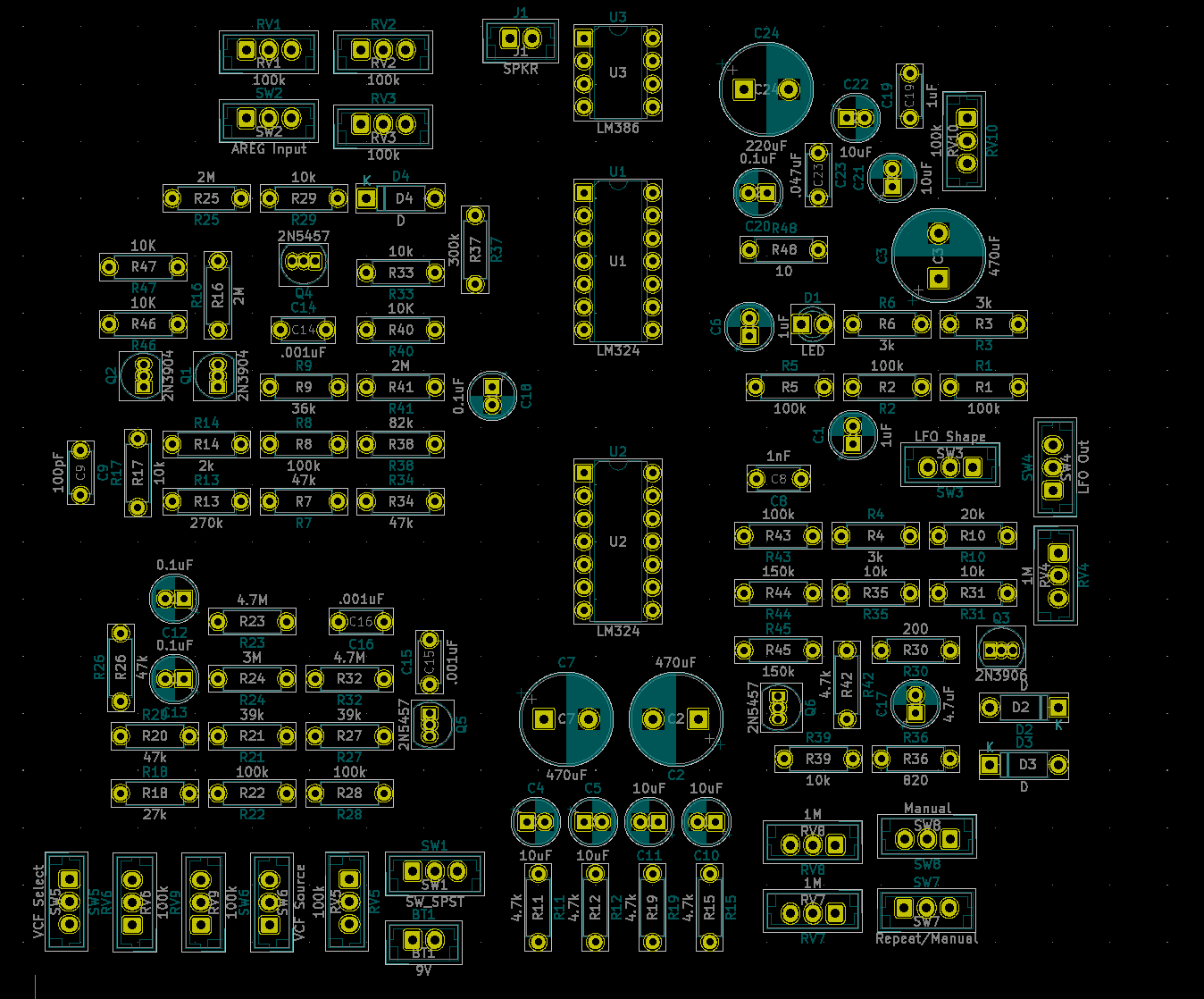
Now it’s time to lay out the footprints
Switches
Toggle Switch
https://www.amazon.com/MTS-101-Position-Miniature-Toggle-Switch/dp/B0799LBFNY/ref=pd_bxgy_img_1/146-9475865-9998724?pd_rd_w=RWoFK&pf_rd_p=6b3eefea-7b16-43e9-bc45-2e332cbf99da&pf_rd_r=37BBPKJACKR5SSPRGD5K&pd_rd_r=fb22504d-e1b7-4af9-9c06-284bf44bdfc6&pd_rd_wg=0sg0Y&pd_rd_i=B0799LBFNY&psc=1
Rocker Power Switch
https://www.amazon.com/dp/B08DKDWKPY?pd_rd_i=B08DKDWKPY&pd_rd_w=7GHH4&pf_rd_p=cc7afcc5-25bd-41a6-9934-4067a293ee62&pd_rd_wg=LyEq9&pf_rd_r=SZESXNAXYMBE93ZTZWDG&pd_rd_r=9f397944-0fd8-43dc-8423-9f246b4bff4e
this one has 2 pin ON/OFF, 3 pin ON/ON and 3 pin ON/Off/ON
10, 11, 101
Switch List
Power Switch: 10
LFO Shape: 10
VCO AREG Input: 10
LFO Select: 11
AREG Repeat/Manual: 11
VCF Select: 11
VCF Source: 11
Totals
11: 4
10: 3
For the footprint on the switches and pots, I can’t just find the pot itself. I’m going to have to run wires off the board up to the front panel.
So I’m thinking I’ll have to design footprints specifically for the wiring jump
It’s either that or I use the JST connectors I used on the 3D Printer. Mount female ports and then attach male ports to the potentiometers. That would make the whole system just a bit more modular and lend itself more to repairs
Checking the book for advice on cable management, signal interference, etc.
Nothing relevant in the book on signal interference. I don’t like the way he sets up the front panel at all
Potentiometer
1M: 3
RV4
RV7
RV8
100k: 7
RV1
RV2
RV3
RV5
RV6
RV9
RV10
Different Pot Link
https://www.amazon.com/OCR-Potentiometer-Assortment-9Values-Terminal/dp/B07YB11Q6W/ref=sr_1_6?crid=1TNCRHN4833I5&keywords=potentiometer+1M&qid=1646936875&sprefix=potentiometer+1m%2Caps%2C109&sr=8-6
https://www.amazon.com/HiLetgo-Single-Joint-Potentiometer-Variable-Resistors/dp/B00N1ZJ0JS/ref=sr_1_1_sspa?crid=1TNCRHN4833I5&keywords=potentiometer+1M&qid=1646936875&sprefix=potentiometer+1m%2Caps%2C109&sr=8-1-spons&psc=1&spLa=ZW5jcnlwdGVkUXVhbGlmaWVyPUE3Rk1OWU9KNFE4RkUmZW5jcnlwdGVkSWQ9QTEwMzU1MTcxT0dFNUNaSUFNTk1YJmVuY3J5cHRlZEFkSWQ9QTA5NzUxNTkxR0RRUEpJVTJPSDJPJndpZGdldE5hbWU9c3BfYXRmJmFjdGlvbj1jbGlja1JlZGlyZWN0JmRvTm90TG9nQ2xpY2s9dHJ1ZQ==
https://www.amazon.com/HiLetgo-Single-Joint-Potentiometer-Variable-Resistors/dp/B07VJYH29F/ref=sr_1_1_sspa?crid=1TNCRHN4833I5&keywords=potentiometer%2B1M&qid=1646936875&sprefix=potentiometer%2B1m%2Caps%2C109&sr=8-1-spons&spLa=ZW5jcnlwdGVkUXVhbGlmaWVyPUE3Rk1OWU9KNFE4RkUmZW5jcnlwdGVkSWQ9QTEwMzU1MTcxT0dFNUNaSUFNTk1YJmVuY3J5cHRlZEFkSWQ9QTA5NzUxNTkxR0RRUEpJVTJPSDJPJndpZGdldE5hbWU9c3BfYXRmJmFjdGlvbj1jbGlja1JlZGlyZWN0JmRvTm90TG9nQ2xpY2s9dHJ1ZQ&th=1
https://www.amazon.com/Knurled-Insert-Potentiometer-Control-Switch/dp/B07F2768F5/ref=sr_1_4?crid=2SG8UXKNPSFRE&keywords=potentiometer+knobs&qid=1646936959&sprefix=potentiometer+knobs%2Caps%2C102&sr=8-4
Capacitors
Ceramic/NP Capacitors
5mm Lead Spacing, 7 total in the system
C8
1nF
https://www.digikey.com/en/products/detail/vishay-beyschlag-draloric-bc-components/K102K10X7RF5UH5/2356873
C9
100pF
https://www.digikey.com/en/products/detail/vishay-beyschlag-draloric-bc-components/K101J15C0GF5TH5/286496
C14
1nF
C15
1nF
C16
1nF
C19
1uF
https://www.digikey.com/en/products/detail/vishay-beyschlag-draloric-bc-components/K105K20X7RF5TH5/2820552
C23
470nF
Electrolytic/P Capacitors ( by module) (17 total)
4 5mm Spaced
13 2mm Spaced
PSU (6)
Ref
Val
Lead Spacing
C2
470uF
5mm
C4
10uF
2mm
C5
10uF
2mm
C7
470uF
5mm
C10
10uF
2mm
C11
10uF
2mm
AREG (1)
C17
4.7uF
2mm
LFO (3)
C1
1uF
2mm
C3
470uF
5mm
C6
1uF
2mm
VCO (1)
C18
0.1uF
2mm
VCF (2)
C12
0.1uF
2mm
C13
0.1uF
2mm
AA (4)
C20
0.1uF
2mm
C21
10uF
2mm
C22
10uF
2mm
C24
220uF
5mm
Spent a few hours routing the PCB. It’s the largest and most complex board I’ve tried to route so far. Everything I try to do feels like I’m just making a mess of the whole thing. I’m wondering what methodologies people apply to make themselves feel like they’re not just stringing everything together at random?
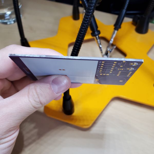
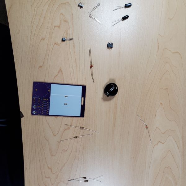
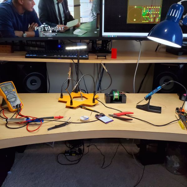
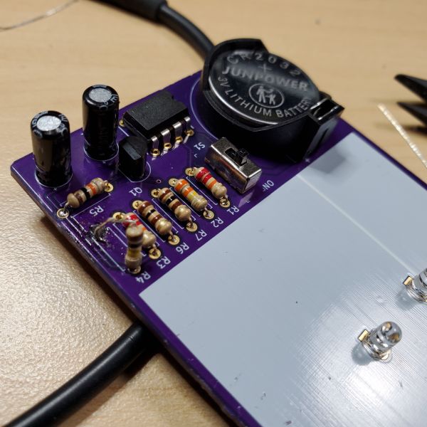
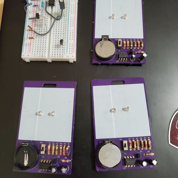
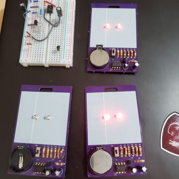
555 Badge PCB Build
I’m realizing I’m not actually very good at soldering and desoldering. I figured this would come up, but I should probably spend a few days to a week practicing advanced soldering techniques so this doesn’t become a point of frustration or limiting factor again. I messed up 2/3 boards and then made the third one with Angel and everything worked on the third one.
On the second one, I actually put the 555 in backwards, and it still managed to turn on, but wouldn’t do the fade animation the whole board was designed for.
For the first one, I had a bad 100k resistor that I didn’t check & test before I put it in, and couldn’t manage to get it out and put a new one into the hole, because I couldn’t clear the solder. So that’s the point that made me feel like I need to improve those skills some more.
I’m guessing it would be fun and worthwhile to just buy some solder-it-together kits for kids to practice. I also bought a SMT soldering practice board a while back, but I didn’t really take the time to learn to do it right.
Resoldering/Desoldering equipment, especially ICs I think is a core skill for making useful products out of scrap equipment