
Project Summary (Technical Overview):
Et et voluptas quis sit tempore tempore. Consectetur quia incidunt doloremque molestias animi doloribus veniam. Totam sunt esse aliquid sit. Et deserunt et enim nobis consequatur laboriosam eos eos. Deserunt dolor quos vel recusandae at sit.
Eum et quia alias fuga. Sint qui sit modi. Provident error officia minus ratione. Atque doloribus laborum delectus est. Nihil ad saepe quidem dignissimos ex est velit eveniet.
Voluptatem et minima optio ex qui. In eum sit nihil et. Illo et ipsam voluptatem hic officiis sapiente.
Quidem eum voluptatem et. Optio voluptas vitae ut tempora voluptate. Porro nobis et earum nisi magnam.
Quas et veniam omnis. Et est id suscipit ipsa nulla nam odit. Iusto in sed qui eos aut quod. Quia ut quis repellendus reiciendis voluptates ipsa est.
Final Project Pics
Project Summary (Personal Overview):
Et et voluptas quis sit tempore tempore. Consectetur quia incidunt doloremque molestias animi doloribus veniam. Totam sunt esse aliquid sit. Et deserunt et enim nobis consequatur laboriosam eos eos. Deserunt dolor quos vel recusandae at sit.
Eum et quia alias fuga. Sint qui sit modi. Provident error officia minus ratione. Atque doloribus laborum delectus est. Nihil ad saepe quidem dignissimos ex est velit eveniet.
Voluptatem et minima optio ex qui. In eum sit nihil et. Illo et ipsam voluptatem hic officiis sapiente.
Quidem eum voluptatem et. Optio voluptas vitae ut tempora voluptate. Porro nobis et earum nisi magnam.
Quas et veniam omnis. Et est id suscipit ipsa nulla nam odit. Iusto in sed qui eos aut quod. Quia ut quis repellendus reiciendis voluptates ipsa est.
Project Cost Breakdown: $400
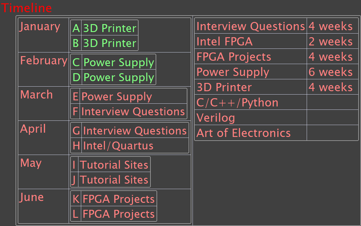
Project Timeline Breakdown: 4 Months
Project Gallery
Project Notes
2022-C
Analog Synth LTSpice Simulation
9 modules
Searching online I managed to find this website, which has a 18MB expanded library and 25MB expanded examples folder for LTSpice.
http://bordodynov.ltwiki.org/
I came across it while looking for a model for the 2N5457 JFET
That library still didn’t have a 2N5457 though, so I found this off of a forum post
https://forum.allaboutcircuits.com/threads/2n5457-spice-model.184060/
.MODEL J2N5457 NJF(Beta=1.125m Betatce=-500m Rd=1 Rs=1 Lambda=2.3m Vto=-1.372 Vtotc=-2.5m Is=181.3f Isr=1.747p N=1 Nr=2 Xti=3 Alpha=2.543u Vk=152.2 Cgd=4p M=311.4m Pb=500m Fc=500m Cgs=4.627p Kf=1.045e-002f Af=1)
Modeled the power supply, which was easy, and the attack-release envelope generator, which was the first time I felt like I was actually doing something in LTSpice on my own. It’s nice
I’m already seeing things I was struggling to see trying to build irl and measure. For example, the virtual ground I introduced didn’t trigger the 4.5V and -4.5V split until I added a resistor network to actually create it. Also, I noticed right away that the 2N3906 was a PNP, and that it was modeled Upside down compared to the schematic.
I also was able to make good use of the .param setup for potentiometers, and the .model declaration for JFETs. All in all, the AREG worked pretty much first try.
For example, I can see the voltages and currents through every device pretty much instantly, and so I figured out the 4.7uF capacitor that’s feeding into the JFET’s gate is the thing that primarily determined the Time Constant of the AREG
This means that I could potentially pick a different cap value and then use 100k potentiometers instead if need be. The possibilities are endless and I can actually see them now.
Switching the AREG circuit between manual and auto, and then adjusting the pot values is giving me a crazy amount of insight that matches up with what I was hearing before. I’m simulating the button press with a periodic, short, pulse to BP
I finally figured out why the LFO never was able to produce the differentiated graph. It can be produced not by switching the switch that claims to produce it in the design, but by taking the voltage differential between the two output channels
the diagram says differentiated output is active on the switch, but shorting the capacitor doesn’t do anything. the differential trace is found in the voltage difference between the square wave and the exponential wave
It seems like I can actually cut out the capacitor entirely C8 1uF
Having some bug issues with the 2N5457 model I’m using that says my timestep is too large to simulate it properly. It usually goes away if I just run it again. I have to model the thing for some good 15 seconds so far to make sure it’s running stable. Honestly, this is probably 10-20x faster than breadboard debugging and measuring, which I’m happy about.
I will need to find a new model for the 2n5457 in order to continue debugging this thing properly
Stopping today on the 4/9 VCO Exp Mixer
I’m getting a weird jagged waveform that seems to source at the open end of AA, the audio amplifier, so I’m going to build that circuit, connect it, and see if it goes away and the VCO/Mixer fixes itself
° – ALT 0176
Breaking down the JFET Model
https://www.youspice.com/spice-modeling-of-a-jfet-from-datasheet/
JFET Available Parameters
Parameter
Description
Unit
Default Value
CurrentValue
DataSheet
AF
Flicker Noise Exponent
no unit
1.0
1
ALPHA
Ionization Coefficient
1/V
1e-006
2.543u
BETA
Transconductance Coefficient
A/V^2
0.0001
1.125m
BETATCE
BETA exponential temperature coefficient
%/°C
-0.5
500m
CGD
Zero-bias gate-drain p-n capacitance
F
1e-012
4p
CGS
Zero-bias gate-source p-n capacitance
F
1e-012
4.627p
FC
Forward-bias depletion capacitance coefficient
no unit
0.5
500m
IS
Gate p-n saturation current
A
1e-014
181.3f
ISR
Gate p-n recombination current parameter
A
0
1.747p
KF
Flicker Noise Coefficient
no unit
1e-018
1.045e-002
LAMBDA
Channel-length modulation
1/V
1e-006
2.3m
M
Gate p-n grading coefficient
no unit
0.5
311.4m
N
gate p-n emission coefficient
no unit
1
1
NR
Emission coefficient for ISR
no unit
2
2
PB
Gate p-n potential
V
1
500m
RD
Drain ohmic resistance
Ohm
1
1
RS
Source ohmic resistance
Ohm
1
1
VK
Ionization Knee Voltage
V
1
152.2
VTO
Threshold Voltage
V
-2.0
-1.372
VTOTC
VTO Temperature Coefficient
V/°C
-0.0025
2.5m
XTI
IS Tempearture Coefficient
no unit
3.0
3
I can’t seem to find my way around the instability in the circuit that causes the JFET to diverge and oscillate
http://musicfromouterspace.com/analogsynth_new/NOISETOASTER/NOISETOASTER.php#SCHEMPG1
I’ll try building it up again using the all in one schematic and referencing the webpage, but if I can’t figure it out and get stuck at the same place I’m dropping this
https://www.electronicspoint.com/forums/resources/how-to-deal-with-lt-spice-error-messages.14/
Slowly but surely figuring it out
The Singular Matrix error seems to indicate a portion of the circuit doesn’t have a pathway to ground
The circuit is based around a 9V battery being used as a +4.5/-4.5V source with a virtual ground in between
The simulator keeps having instability problems where it can’t process certain subcircuits because it thinks they have no path to ground, because they’re touching virtual ground when it expects actual ground (- terminal of the 9V) or vice versa
Thankfully, I’m starting to get the hang of adding a few components and debugging the circuit and figuring out what’s crashing the sim and why. Usually it’s fixed by adding or swapping the “grounds”
I thought it was an issue with the 2n5457 at first because it’s the component that diverges, but i don’t think so anymore.
I also thought it was an issue with the fact that LTSpice doesn’t do polarized capacitors, which led to me adding diodes to my capacitors to see if it could fix the issue, it didn’t. I think it’s the case that all Spice simulators completely ignore capacitor polarity, and I haven’t found any tutorials on how to simulate that quality either
Super critical information…
Simulation is much more stable after replacing the opamps with LM324_AB version
1:56 secrets in plain sight
adding in the Synth feels like an inflation of the project, since it’s eating up a lot of time. But at the same time, I’m getting a lot of experience debugging LTSpice and getting it to do what I want. But I am frustrated that the Synth, no matter how I try to approach it gives me a ton of issues. I’m hoping that I’ll be able to finally overcome it and get it it to work in a way that satisfied me. This thing has defeated me before and I really want to turn the tables on it. I’m learning a lot either way though. I can tell I’m getting a better intuition for circuit analysis, and how op amps and transistors work
Slowly but surely figuring it out
The circuit is based around a 9V battery being used as a +4.5/-4.5V source with a virtual ground in between
The simulator keeps having instability problems where it can’t process certain subcircuits because it thinks they have no path to ground, because they’re touching virtual ground when it expects actual ground (- terminal of the 9V) or vice versa
Thankfully, I’m starting to get the hang of adding a few components and debugging the circuit and figuring out what’s crashing the sim and why. Usually it’s fixed by adding or swapping the “grounds”
I thought it was an issue with the 2n5457 at first because it’s the component that diverges, but i don’t think so anymore.
I also thought it was an issue with the fact that LTSpice doesn’t do polarized capacitors, which led to me adding diodes to my capacitors to see if it could fix the issue, it didn’t. I think it’s the case that all Spice simulators completely ignore capacitor polarity, and I haven’t found any tutorials on how to simulate that quality either
Since the circuit isn’t behaving as it should, starting around the VCO, I’m going to rebuild it using the GND node as the terminal of the battery BN, and replacing the Virtual Grounds with a tag VG
Finally got a ramp coming out of the JFET#2 with the new layout, but the simulation is still crashing frequently
Spent a few more hours today building out the circuit again. I was able to get the RAMP function working properly. The big issue on the previous builds was that I was connecting the 2M JFET gate resistor to Virtual Ground instead of BN. When that happens, the RAMP function is unable to work properly. I made that change because without it the simulator would crash consistently. It seems like something about the RAMP function’s production is what crashes the simulator. The spike in the gate voltage that causes the JFET to short the capacitor seems to be the thing breaking the simulation.
Moving on from that, every other portion of the synth seems to simulate just fine. Since I can’t get the VCO to produce a stable, adjustable output that I expect, I can’t really test the VCF or VCA in a meaningful way. I’m not sure what I can do to get the VCO circuit to work.
I think I’ll have to go in and replace some of the components with ideal components to get it to work.
I suppose I can just get the ramp function’s general specs and then simulate a ramp output in order to move forward. but I’d really like to get the VCO working without complaint. That’s the main victory I’m working towards here.
Rebuilt the VCO in isolation and it ran just fine with a generic JFET.
At 4.5V control voltage (pot at 50dev) the frequency is just about 12.5 kHZ
At 2V control voltage, frequency is 1.42kHz
after much trial and error I have figured out that the VCO is working as intended, but it has a mechanism where it exponentially converts small fluctuations into large current sinking into a cap and then switching the JFET to discharge, all to create a ramp wave. The higher the frequency of the ramp wave, the more computationally intensive the simulation becomes. The only way to continue working on the circuit in a meaningful way and verify its functional is to lower the control voltage/frequency of the VCO as much as I can
The speed of the simulation corresponds to the frequency of the ramp. Something about calculating these ramps is extremely CPU intensive and Spice hates it
Moving forward I’m going to have to keep the VCO Control voltage at a really low number for simplicity of simulation. I’ve already verified that it works at higher voltages/frequencies in isolation.
If I’m going to get the whole synth to run at once in a simulation without breaking it into submodules that’s the only way I see this working.
I’m going to have to save a copy of the VCO as its own base circuit and then build up the rest around it, and hope it doesn’t crash
Example: At 7V control voltage, VCO frequency is 41kHz, but sim speed is around 7.7ms/S, which means it would take 20 minutes just to simulate my 10S interval. Maybe the extremely slow simulation wasn’t the result of a bug, but it was functioning correctly, and it just takes that long to process..
Running the 7V for 2 seconds test gets my CPU up to 85C, 46% load, so I’m guessing that’s literally what’s been going on.
So, the system crashes even with the isolated VCO at 1V and 1.5V. 2V seems to be the lowest stable Voltage
This is with the default value JFET too. Not using the 2N5457.
After inputting the 2N5457, the sim crashes at 2V, seems to run fine at 4V. But then the sim takes longer becuase of the increased frequency
doing a visual comparison of the 2N5457 and the stock JFET’s ramp at 4V ~ 5kHz. If the waveforms are similar, I’m using the stock
2N5457
5kHz
870mV
Stock
8.5kHz
500mV
33ms/S
The difference is bigger than I was expecting. It’s good enough though
Got the SQW and RAMP wave working for a full 2S at a control voltage of 4V with the 2N5457 model. Sim speed is about 22ms/S
Added the LFO circuit and was still able to run 2S. This one doesn’t have a JFET
The B connection to the VCO does not work in the slightest. I also had to tune the set voltage for that opamp, and had to give caps an IC so they came precharged in order for the sim not to crash
After adding the AREG, which has another JFET, I’m still managing to complete the simulation, but it’s running at about 16ms/S
Next is adding the LFO and AREG to the input of the VCO, which I have a feeling will just wreck the entire thing
Adding the LFO, I was able to confirm that it works when the LFO signal is injected into the summing amplifier, but it’s unable to finish the sim. The response was as expected though. The frequency of the ramp shifted instantaneously once the LFO dropped
LFO injected into VCO input
ARG injected into VCO input
I was able to briefly simulate all three at once, but there’s no chance it’ll work consistently. I’m readjusting the VCO to be control voltage only
Moving onto the VCF
Verified that the VCF is working as intended using the pure ramp as an input signal.
Twisted around the pot values and achieved some different waveforms
Inserting the AREG and seeing how to plays into the filtering mechanism. The ramp input has no AREG component, but that is actually an option in the real synth so the exercise is still constructive.
Got the whole thing working
Built out the WNS. It’s strange to simulate noise, but I got it working at a level strong enough to influence the output waveform.
After that, I just dropped in the AA and it just worked. It has a singular matrix error after about 130-200ms, but its enough time for me to verify that it’s working as intended, which I’m happy about.
The last version of the synth that seems guaranteed to work is VCO-VCF – VCA – ARG working. Everything after that has a crash condition
Now that I have the whole synth functioning in one module, I’m trying to clean it up and optimize it a little.
One thing that seems to help is connecting cross-module signals via behavioral voltage sources rather than using tags. That seems to provide some isolation they need
I actually managed to complete a full 2s run with the new BV flag setup
Finally Complete!
Reorganized the schematic, added boxes and labels
Confirmed stability
Printed an export of the schematic
Cleaned up drafts and file versions organization
Added final working file to a .rar
All buttoned up and ready for presentation
I’ll have to collect all the snips I posted on discord and use those as lab pics for this sprint
Have two functional copies. One runs way faster than the other because I cut out the white noise simulator
The fastest I can get a stable version to run a simulation is about 12ms/s, which has made this whole thing pretty rough
I also only just realized my project folder is 2GB because this thing manages to produce 200MB of data after a full two second run. Something about that ramp wave generator really doesn’t get along with SPICE
Next is to breadboard it again now that I have an effective sim to check against, and then build out the PCB
2022-D
Synth Breadboard Layout
Set up Fritzing
Fritzing is Open Source, but they ask for a donation and don’t take no for an answer
This means you have to download it on github and build it yourself
But to build it you need Qt installed
What the hell is Qt?
Seems to be a C++ based GUI/App development platform. They have an enterprise license but are still open source. Their stuff looks pretty slick
Finished installing Qt. Having trouble building the App according to the github’s instructions.
I think I don’t have g++?
Picking this up tomorrow
https://www.sefidian.com/2020/05/09/installing-g-c-compiler-on-windows/
https://github.com/fritzing/fritzing-app/wiki/1.2-Windows-notes
Had some free time since work was slow. Got super mad trying to figure out how to build this thing. I stopped caring and just paid the $8 euros or whatever for the windows installer.
They totally got me lol
After building out the entire VCO and AA circuits on the main breadboard, and neither of them working, I modified the AA until it worked and then rebuilt the VCO circuit on a different breadboard entirely.
I’m using jumpers now because the solid core cables are just too much hassle to deal with and I’d rather deal with signal interference than have to spend 2 hours every day hurting my fingers against a stiff breadboard slot clip
After I got the AA working, an interesting thing happened. When adjusting the pot with a screwdriver that controls the input signal’s volume, the metal of the screwdriver made contact with the body of the pot and then the screwdriver acted as an antenna, and managed to pick up some rock music.
I’ve read before that you can accidentally made an AM radio playing with op-amps, so I’m guessing I did that, or something similar. The noise was much louder when I was also touching the antenna with my finger. I’m not sure why. It’s pretty cool though. Easily avoided.
After rebuilding the VCO on the smaller breadboard I was able to get the ramp wave out of it, but I noticed that the frequency was way too high, even at the bottom of the range. I figured I might be able to adjust the feedback op-amps set voltage, so I used a pot and swung it around 5.8V. This caused some clipping on the top of the ramp wave, so I tuned both the input voltage and the feedback set voltage until I could get a properly sharp ramp wave across the full range
After I got that, I took some measurements, and came up with some resistor divider values that will allow that to hold without a pot, and that worked fine.
As for the frequency of the ramp wave being way too high, I figured that it could be adjusted by changing the flat mod depth resistor after the input voltage pot, and I was right.
By increasing that resistor, I lowered the current heading towards the op-amp input, and that managed to increase the frequency. So I started lowering it until it got to a point where the ramp wave could collapse. The most stable value I found was 47k, and that allows me to produce sub-kHz frequencies.
After I was satisfied with the voltage adjust/frequency adjust for the VCO, I started tying in the LFO and AREG signals, which worked as intended. Just fine actually. When I first built this thing, each knob on each pot was a mystery, but now I have a deeper understanding of what turning that knob is actually doing to specific voltages and currents inside the circuit, and so the whole thing is a lot more intuitive.
There’s still some interference and feedback and static. I’m hoping these go away once I get the thing onto a PCB and there aren’t as many wires running over eachother.
I don’t have as many pictures for this breadboard layout yet, but I will probably take a lot of the waveforms at the end once it’s working
All that’s left at this point is building the Square wave section of the VCO, and then the VCF, which is technically the biggest subcircuit.
Following what I’ve learned from the VCO, I’m going to build the VCF on a separate breadboard as well. I’m hoping this goes as smoothly as the VCO.
Once I have everything Functional on a small network of deeply interconnected breadboards, I plan on extracting each pot from its location, placing it onto a blank breadboard, and using that as a mock front panel before routing and ordering the boards.
It’s also important that I compile all the slight changes to the circuit, as well as the slight errors I’ve found in the schematic. Many resistor values have been changed in the breadboard prototype simply because I don’t have those values and am not going to waste 4 resistors building them. I’ve found some missed connections on the KiCAD schematic as well. Which is good, because that means building the breadboard synth for the THIRD TIME wasn’t a waste of time.
I’m hoping to have this whole thing buttoned up inside a nice box in the next 2-3 months and then I can finally put this Synth to rest. The first time I tried to build it in Nov 2020, I had no idea what I was looking at. Sometimes I wish it didn’t take this long or I never tried lol. But, perseverance and time make the magic happen
Synth PCB Layout
Building Schematic in KiCAD
Spent today’s lab session building out the LFO and AREG on breadboard, both work fine.
Next is the VCO, which I’ll set up with just the voltage control first to verify, now that I know how it’s supposed to work. Once I’ve confirmed that it works, I’ll tap in the LFO and AREG signals and test the combination
Found some bugs in the KiCAD Schematic as well
I should come up with a functionality checklist for the breadboard Synth
One of the most important features that I want to ensure works on the finished product is the line out feature. I need to make sure the finished circuit can actually tap out into an aux jack and go into a computer and get recorded via Audacity. That means the synth can actually connect to a digital system and get sampled, which is important to me.
I’m hoping to be able to distribute a few copies of the finished synth once the whole thing is completed. I’m guessing that, if I want to make that the distribution present for christmastime this year, I’m going to have to do 2-3 revisions of the PCB to add features and package it properly.
One thing I’m not quite prepared for is the casing. It’s easy enough to make a housing for a PCB, but since I have to make a front panel for the whole thing, I’m not sure if 3D Printing will be appropriate. The dimensions will be fine and the pots can be rigidly mounted, but I don’t know how to mask a UI onto the front panel of a 3D printed plane like that. I’m sure there are answers online
Further, for power supply, I started thinking about using a rechargable LiPo cell. But I’m pretty sure those are almost all 4.5V or below, which means I would have to use a Boost Converter which might affect audio quality with spiking in the power supply. On top of that, the current draw would be higher than normal. I’m guessing the synth is pretty low power. I think it only draws 15-20mA when it’s working, but that speaks nothing of the audio amplification, which could go up to a 1/4W.
.25W / 9V = 27 mA
20 mA + 27mA = 47 mA ~= 50mA
9.6V LiPo cell 2000mAh: 40 hours of synth time
That’s wrong. A quick sim shows the peak current going through the speaker will be 780mA 2pk. So the amplitude is about 390. The RMS current is 0.7071*390=275mA
275+20 = 300mA
300mA on a 9.6V LiPo cell 2000mAh: 6 hours
I could design it with both a barrel jack for 9V AND a 9V Battery slot, but I don’t think that’s worthwhile just yet. It’s probably cheaper than adding a rechargable cell to each instance, so I may get there in the future, but for now I’m going to just assume it’s plugged into the wall.
I’m thinking it might be worthwhile to make a mockup of the front panel now, before I order a PCB, so that I can ensure that everything will actually work as intended. It’s one thing to experience a bunch of boardboard switches and pots as functional. It’s another to make a tangible UI to the project that can be adjusted more intuitively.
Design a sheet of PLA with holes in it for the pots
Design some handles for the tiny pots? or just use screwdrivers for this
Design holes for the switches as well
Mask it with a sheet of paper for labeling, or use the label maker
Mount everything into the PLA Panel, solder wires that can connect back to the breadboard
Follow the advice of the book on signal interference
I could also just get a second breadboard and jump everything over to the original breadboard, and have only UI front panel components on the second breadboard. That would be just as good with significantly less intermediate design work. It won’t change the fact I’ll have to design a front panel sooner or later though.
For the breadboard as I left it, I have the LFO and the AREG working. Next is to make an unmodulated VCO circuit, which will take a while. Then the AA, to verify that the VCO can produce an audible waveform. From there, I’ll have a basic functionality that I can then tie in the AREG and LFO to, to ensure that all the features work
Once I have completed the checklist via the breadboard, then I can move onto designing a front panel mockup. Once the breadboard synth and the front panel mockup are satisfactory, I can move onto designing the PCB in earnest, with the confidence that I have a fully functional prototype. That will be the more fun part for sure.
I’ve been thinking a lot lately about how the synth is probably a more complex project than the power supply I’m using it to prepare for. But that’s fine. This is worthwhile engineering work for me. I’m going to beat this Synth and not let it frustrate and overwhelm me. And then I’ll get to share that victory with others
Notes on Schematic Changes from Breadboard Tweaking
Resistor on Exp.Wave output on LFO changed from 75k to 20k
Changed Flat Mod Resistor on Voltage input to VCO (VCO Freq) from 75k to 47k
Connected JFET properly on AREG (not connected on schematic)
Skipped Sync Effect on LFO. Still needs to be tested. Currently using a simple voltage divider at a tuned voltage of 5.85V, with a source voltage of 9.15V
Put Coupling Capacitor on AA ahead of the pot
On AA, LM386 Pin 2 and 4 are not connected to ground in schematic
Synth Schematic Performance Checklist
PSU
Maintains a virtual ground of 50% dV
AREG
Produces Attack-Release Envelope
Repeat/Manual function
LFO
Adjustable Low Frequency
Produces Square Wave
Produces Smooth Wave
Produces Spike Wave
All output waves selectable to LFO node
VCO
Voltage Controlled Frequency of Ramp Wave
Ramp Wave converts to Square Wave
Modulation by AREG
Modulation by LFO
Sync Effect Functional
VCA
VCA amplifies output signal according to AREG signal
VCA Bypass switch functional
WNS
White Noise is audible when fed directly to output
White noise has an audible effect when mixed in
AA
AA Can properly drive the speaker
AA has meaningful volume adjust
AA can run for extended duration without overheating or damaging anything
AA can effectively line-out to an external speaker
AA can effectively line-out to an external computer and be sampled via audacity without incident
Summary
VCA is basically pointless and I’m going to take it out of the circuit again, like I did last time.
VCF is extremely finnicky and so I’m going to add a multi switch so the signal that gets amplified from
RMP
SQW
VCF
Removing the VCA and the WNS, both are shit. Also skipping the LFO- B Sync Effect
2022-E
Synth R1 PCB Layout
After adjusting the schematic with the changes I found and discovered on the breadboard, it’s time to assign footprints and get moving on the board.
I’m about two weeks behind schedule now due to having to spend the last two weeks out in the field for work, and because I decided to include the Synth as another project before moving onto the power supply. Once the power supply is finished, I’m going to pore through the interview questions, and that should be sufficient to conclude the bootcamp and move on to something more specific
I do find myself wanting to push through and get through all this so I can read AoE cover to cover. I’m gonna have to do it eventually.
List of changes:
Removed input/bias resistors from pin 3 of LM386
Changed VCO depth for voltage source to 47k
Removed Sync Effect switch and set up simple voltage divider on VCO
Flipped Bypass capacitor on LM386 orientation
Deleted VCA
Deleted WNS
Now it’s time to lay out the footprints
Switches
Toggle Switch
https://www.amazon.com/MTS-101-Position-Miniature-Toggle-Switch/dp/B0799LBFNY/ref=pd_bxgy_img_1/146-9475865-9998724?pd_rd_w=RWoFK&pf_rd_p=6b3eefea-7b16-43e9-bc45-2e332cbf99da&pf_rd_r=37BBPKJACKR5SSPRGD5K&pd_rd_r=fb22504d-e1b7-4af9-9c06-284bf44bdfc6&pd_rd_wg=0sg0Y&pd_rd_i=B0799LBFNY&psc=1
Rocker Power Switch
https://www.amazon.com/dp/B08DKDWKPY?pd_rd_i=B08DKDWKPY&pd_rd_w=7GHH4&pf_rd_p=cc7afcc5-25bd-41a6-9934-4067a293ee62&pd_rd_wg=LyEq9&pf_rd_r=SZESXNAXYMBE93ZTZWDG&pd_rd_r=9f397944-0fd8-43dc-8423-9f246b4bff4e
this one has 2 pin ON/OFF, 3 pin ON/ON and 3 pin ON/Off/ON
10, 11, 101
Switch List
Power Switch: 10
LFO Shape: 10
VCO AREG Input: 10
LFO Select: 11
AREG Repeat/Manual: 11
VCF Select: 11
VCF Source: 11
Totals
11: 4
10: 3
For the footprint on the switches and pots, I can’t just find the pot itself. I’m going to have to run wires off the board up to the front panel.
So I’m thinking I’ll have to design footprints specifically for the wiring jump
It’s either that or I use the JST connectors I used on the 3D Printer. Mount female ports and then attach male ports to the potentiometers. That would make the whole system just a bit more modular and lend itself more to repairs
Checking the book for advice on cable management, signal interference, etc.
Nothing relevant in the book on signal interference. I don’t like the way he sets up the front panel at all
Potentiometer
1M: 3
RV4
RV7
RV8
100k: 7
RV1
RV2
RV3
RV5
RV6
RV9
RV10
Different Pot Link
https://www.amazon.com/OCR-Potentiometer-Assortment-9Values-Terminal/dp/B07YB11Q6W/ref=sr_1_6?crid=1TNCRHN4833I5&keywords=potentiometer+1M&qid=1646936875&sprefix=potentiometer+1m%2Caps%2C109&sr=8-6
https://www.amazon.com/HiLetgo-Single-Joint-Potentiometer-Variable-Resistors/dp/B00N1ZJ0JS/ref=sr_1_1_sspa?crid=1TNCRHN4833I5&keywords=potentiometer+1M&qid=1646936875&sprefix=potentiometer+1m%2Caps%2C109&sr=8-1-spons&psc=1&spLa=ZW5jcnlwdGVkUXVhbGlmaWVyPUE3Rk1OWU9KNFE4RkUmZW5jcnlwdGVkSWQ9QTEwMzU1MTcxT0dFNUNaSUFNTk1YJmVuY3J5cHRlZEFkSWQ9QTA5NzUxNTkxR0RRUEpJVTJPSDJPJndpZGdldE5hbWU9c3BfYXRmJmFjdGlvbj1jbGlja1JlZGlyZWN0JmRvTm90TG9nQ2xpY2s9dHJ1ZQ==
https://www.amazon.com/HiLetgo-Single-Joint-Potentiometer-Variable-Resistors/dp/B07VJYH29F/ref=sr_1_1_sspa?crid=1TNCRHN4833I5&keywords=potentiometer%2B1M&qid=1646936875&sprefix=potentiometer%2B1m%2Caps%2C109&sr=8-1-spons&spLa=ZW5jcnlwdGVkUXVhbGlmaWVyPUE3Rk1OWU9KNFE4RkUmZW5jcnlwdGVkSWQ9QTEwMzU1MTcxT0dFNUNaSUFNTk1YJmVuY3J5cHRlZEFkSWQ9QTA5NzUxNTkxR0RRUEpJVTJPSDJPJndpZGdldE5hbWU9c3BfYXRmJmFjdGlvbj1jbGlja1JlZGlyZWN0JmRvTm90TG9nQ2xpY2s9dHJ1ZQ&th=1
https://www.amazon.com/Knurled-Insert-Potentiometer-Control-Switch/dp/B07F2768F5/ref=sr_1_4?crid=2SG8UXKNPSFRE&keywords=potentiometer+knobs&qid=1646936959&sprefix=potentiometer+knobs%2Caps%2C102&sr=8-4
Capacitors
Ceramic/NP Capacitors
5mm Lead Spacing, 7 total in the system
C8
1nF
https://www.digikey.com/en/products/detail/vishay-beyschlag-draloric-bc-components/K102K10X7RF5UH5/2356873
C9
100pF
https://www.digikey.com/en/products/detail/vishay-beyschlag-draloric-bc-components/K101J15C0GF5TH5/286496
C14
1nF
C15
1nF
C16
1nF
C19
1uF
https://www.digikey.com/en/products/detail/vishay-beyschlag-draloric-bc-components/K105K20X7RF5TH5/2820552
C23
470nF
Electrolytic/P Capacitors ( by module) (17 total)
4 5mm Spaced
13 2mm Spaced
PSU (6)
Ref
Val
Lead Spacing
C2
470uF
5mm
C4
10uF
2mm
C5
10uF
2mm
C7
470uF
5mm
C10
10uF
2mm
C11
10uF
2mm
AREG (1)
C17
4.7uF
2mm
LFO (3)
C1
1uF
2mm
C3
470uF
5mm
C6
1uF
2mm
VCO (1)
C18
0.1uF
2mm
VCF (2)
C12
0.1uF
2mm
C13
0.1uF
2mm
AA (4)
C20
0.1uF
2mm
C21
10uF
2mm
C22
10uF
2mm
C24
220uF
5mm
Spent a few hours routing the PCB. It’s the largest and most complex board I’ve tried to route so far. Everything I try to do feels like I’m just making a mess of the whole thing. I’m wondering what methodologies people apply to make themselves feel like they’re not just stringing everything together at random?
2022-F
Finish Routing Synth PCB and order
R1, R2 Notes
Routed the board about three times now
I’ve tried different methods and I’ve come up with a few design principles that work for me for now, as a beginner
I’m having a lot of success using one layer for vertical traces and one layer for horizontal traces
This becomes a little more complicated in traces that are mostly equal in rise/run & are diagonal.
I feel like Vias are a copout cheater move, so I don’t want to use vias whenever possible, but Tyler told me he’s been enlightened and Vias are fine, good, legal, and necessary
With that as the case, I might be more open to making diagonal runs go in two layers, with vertical, and then horizontal segments
In addition to that, I also route power and signal lines first, then fill in the rest.
I realized about 2.5 routings in that I could use copper pour, but I’m not sure how effective that would be for my purposes
Tyler advised me that any coupling capacitors for the opamps will be basically ineffective if they are too far away, and that I should place them closer. I’m not sure if I’m even ready to worry about something like that right now though.
I’m not sure this whole thing will blow over later on once I print it out.
I’m thinking it might be worthwhile to pass the schematic and final board layout off to hempler and/or tyler so they can review it for me before I print.
If I were to do that, I would take a copy of the original schematic for the Noise Toaster, redline it, and then pair that with the schematic that formed the netlist for the PCB routing.
I would send the schematics to hempler to cross check, and then the pcb layout and the schematic to tyler for layout critique
Along with that, I should mentally prepare myself for the frustration of having to pay for printing this thing like 3x, and to have to solder the whole thing together only for it to not work at all, probably about 3x as well.
As much as I want to minimize the risk of that happening, this is my first complex board and even just routing it I can tell that I’m a total amateur, and there’s a serious at form behind this.
It does make me wonder what kind of crazy AI we have right now that can design something like this optimally and automatically
Along with keeping copper pour in mind for the ground pins, Tyler also warned me that if my ground traces are long, I need to make sure they are fat, or I will end up with Ground Loops. There’s clearly a lot in this area I don’t know about
I can see myself rearranging and rerouting this thing many more times. I can tell each iteration is getting better than before.
It took me a while to accept that it simply takes time to position and rotate each component in a meaningful way to allow the layout to be any degree of effective
The board size is looking around 100mm x 160mm at the moment
R3 Notes
I tried routing using as many vias as I wanted in order to keep all the backside lines vertical and all the frontside lines horizontal. It worked out pretty well. 41 vias total.
I also didn’t route Ground / Net BN and used copper pour at the end to fill it in
As I expected, since the board is taller than it is wide, the copper pour should go on the front side, where the horizontal traces are less complex and less prohibitive
Putting the copper pour on the backside with the green results in some unfinished connections in the ratsnest
That’s the best one yet for sure, so I’m going to redo it once or twice more after positioning the silkscreen names on the board, to polish it up more
I’ll also probably reposition some stuff as well
R4, R5 Notes
After repositioning all the silkscreen reference designators, I also took the time to reorganize some of the components and fit them all into a much denser, more perfectly rectangular footprint. That’s probably the most important thing I did today besides adding a second copper fill
Now there are two copper fills, one on toplayer for BP and one on bottom layer for BN. There were a couple connection points where the copper fill zone didn’t connect every single BN or BP, so I had to go ahead and bridge some of connections before redoing the fill. That didn’t disrupt the flow of the board at all though.
Once I took a look at the 3D Viewer’s render of the board, a lot of stuff started to click, so I rerouted once more to make it lok even better.
I’ve started getting more comfortable using vias very liberally. R5 has 71 vias.
I also have gotten a good enough eye to see how some traces are going to interfere with other traces, but that’s primarily because I’ve gotten very familiar with the problem areas on the board.
Along that line, I took the time to identify all the long distance connections that wrap around the corner of the board and aligned them all so they don’t look as ugly.
On R5 there was one line in that group that I caught too late and would’ve had to redo basically all of the long ones in order to fit it in properly
I also noticed the JST connectors were often flipped or rotated and not facing the same direction. I rearranged things even if that made it more complicated to route, so it would look more polished in the 3D viewer.
As of R5 the 3D view looks solid. Dense and Polished.
The board’s dimensions are around 140x65mm with the extra room for the traces.
I checked on JLCPCB and it costs more to get any board that isn’t 100mmx100mm
I’m at a decent stopping point for it now so I think I’ll pass this onto tyler and ask him to take a look at it so I can move on from this and finally place the order
I feel like I’m quickly developing a skill and appreciation for the creative thinking that an elegant board layout requires. I’m sure it gets even more extreme with high speed signals, more than two layers, and SMT components
PCB Sanity Check Before Ordering
Opened Schematic, Exported Netlist, Imported Netlist to PCB, No changes to the ratsnest.
Now to check the KiCAD schematic against the original schematic and mark changes
Discrepancies
The fake VG on the schematic that connects to the positive end of the op-amps throughout the VCO is actually tied to VG on my schematic
The resistor in the RC on the non-square output of the LFO is listed as 75k on the official MFOS, but it’s 20k on my breadboard and on my schematic and seems to work just fine. Not Changing
Flag “B” removed, LFO sync feature removed
Bypass Cap on LM386 1-8 can be put in either direction. Positive side faces pin 1 on schematics, but is reversed and functional on breadboard
First output resistor on SQR wave is 100k on MFOS schematic, but 10k on KiCAD. Breadboard has 10k, works fine as is. Am interested, but Not Changing.
Second Opamp on VCO has threshold voltage adjusted, no sync effect, just replaced with a voltage divider.
PCB Ordering
JLCPCB Ordering Instructions
https://support.jlcpcb.com/article/149-how-to-generate-gerber-and-drill-files-in-kicad
Gerbers Generated, Drill Map Generated, all layers double checked
Placed order on JLCPCB for a total of $23.73 for 5 boards at 150x75mm
Only thing I didn’t add was mounting holes, which should be fine. I can drill them myself later if I need to.
MFOS Noise Toaster R1 PCB ordered – 3/19/2022
2022-G
Synth PCB
Order Pots and Switches
Soldering plan
Place Order, Print Papers, Set up Station, Pick Parts, Get Moving
Notes from E
Potentiometer
1M: 3
RV4
RV7
RV8
100k: 7
RV1
RV2
RV3
RV5
RV6
RV9
RV10
Switch List
Power Switch: 10
LFO Shape: 10
VCO AREG Input: 10
LFO Select: 11
AREG Repeat/Manual: 11
VCF Select: 11
VCF Source: 11
Totals
11: 4
10: 3
Angel suggested I print out an enlarged sheet of paper, sketch the values onto the zones, and then use that as a holder for all the part placements. Honestly a really good idea. I’m out of black printer ink at the moment though, so it’ll have to be in like, red or something.
I imagine picking out all these components several times over is going to be a huge pain in the ass. I’m guessing I’m going to run low on some stuff and have to order some new ones, especially for the later instances of the board
The JST connectors also need to be built out carefully, because if I miswire them stuff might not work as intended. The pins on the JST’s can be indicated on the piece of paper too, so that’s another point
I wonder how resistors are made, and if one could make an on-demand resistor printer machine. It could print values from 10-10M with some moderate tolerance rating like 5%. You’d punch it in like the coca cola freestyle soda machines and it would just grind and crunch for a second like a vending machine and drop out the custom fab resistor right there.
Something like that would probably be a little harder to pull off with capacitors
I’m not sure if I should use the pots I have access to now as a debug/test tool. It’d be a bit of a waste of the JST connectors, but also lets me fail without having to place yet another parts order in case I do mess up
Probably smart
Lots of soldering today, my soldering stand is still dead in the water… Something to work on later
It just occurred to me that I could save myself an hour by buying some pre-crimped JST-XH 3 pin connectors. I’m not a big fan of buying my way out of problems but like, there’s 15 3-pins here. That’s basically a whole day of work
The connector sets come in sets of 20, so I think I’ll make this first board a test board, and then polish it later, or just solder together a second one
Which means I’ll connect these pots and switches as directly as I can, instead of trying to make a mock front panel
Assembly Notes
I think R13 and R14 are switched on the PCB layout, and I have no idea why, but that may explain the malfunction of the VCO
R13 adn R14 had their reference designators flipped on the schematic, which informed me as to the value of components. So the PCB had them in the correct position, but the schematic instructed me to reverse their positions, which created the error.
After flipping them back, I was able to get the VCO working perfectly.
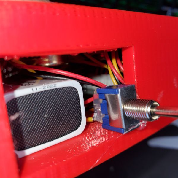
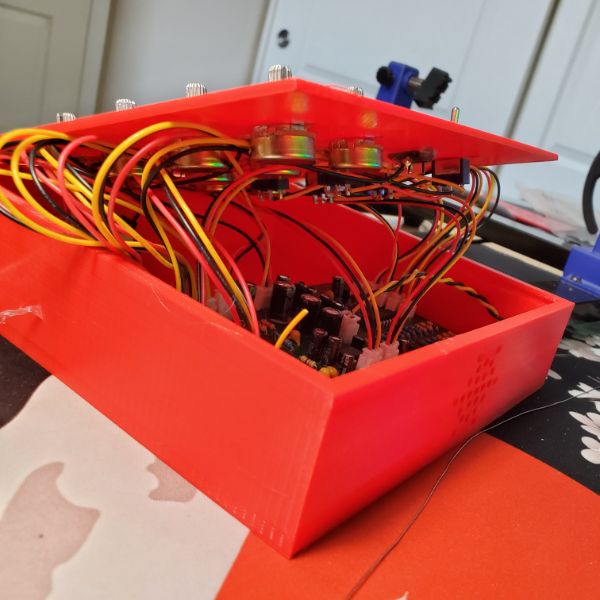
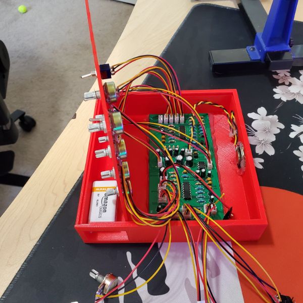
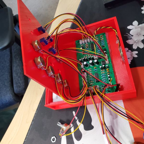
The entire synth is assembled now and it works pretty much perfectly. It’s way more functional and stable/less noisy than the breadboard synth. The only issues I’m having at the moment are, the speaker is absolutely destructively loud unless the volume pot is at like 3%.
I also noticed I’m still picking up some radio signals whenever my hand is in contact with the volume pot.
The AREG pots don’t seem to work exactly as I expect, but I think it’s because the pots are soldered directly on.
I had to disassemble and clean out the solder sucker, and now I can use that in tandem with the copper mesh tape for absorbing solder to desolder components pretty cleanly. That was always an issue before that prevented me from fixing mistakes, but now I can desolder and resolder as much as I want, so that’s nice.
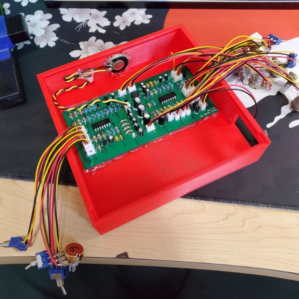
I originally built out the PCB expecting to do a second pass, but it seems like it’d be easier to just desolder the switches I connected directly and add the JST connectors, and make this board the first rendition of the final product.
One thing I neglected to do in the board design was add screw holes to mount the PCB to the casing. I’ll either have to carefully drill them myself, or create a 3D printed snapping mechanism specific to these board dimensions
I replaced the 100k pot in the volume adjust with a 1M pot to try and get the thing to be quiet, and it sort of succeeded, but I noticed signal quality was much higher with the 1M pot, so I’m sticking with it.
I purchased JST-XH connectors off of amazon so I didn’t have to spend hours crimping, but it turns out I ordered JST-XH Mini connectors, so they’re not actually the same as the ones I’ve been crimping by hand, and the inconsistency drives me a little crazy, but the minis are actually more convenient for this case. Something to pay a little more attention to later
Housing and Front Panel Notes
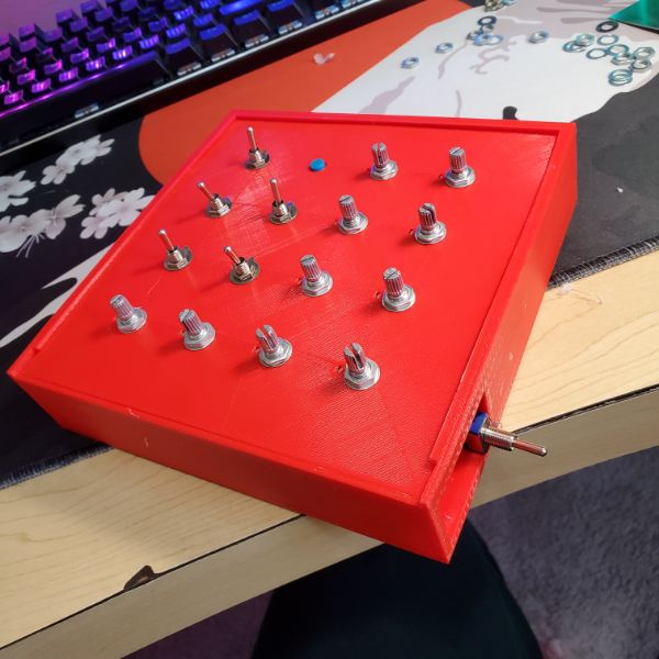
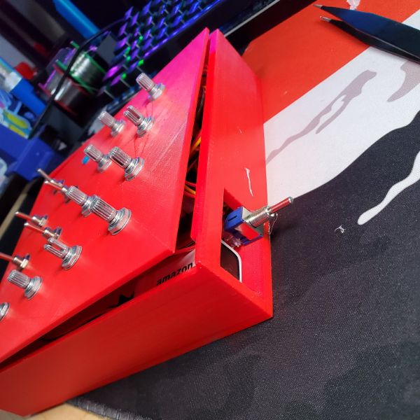
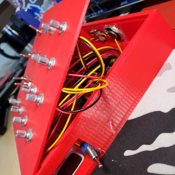
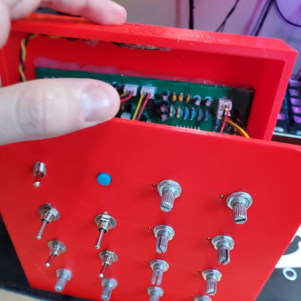
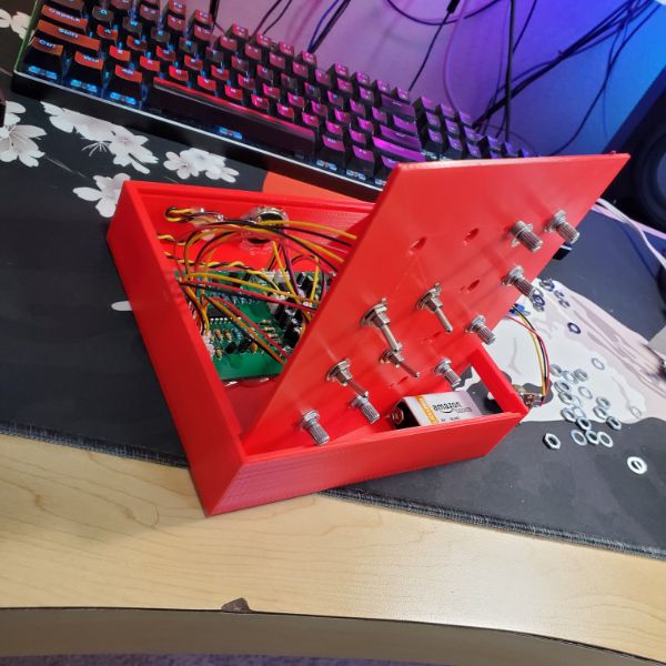
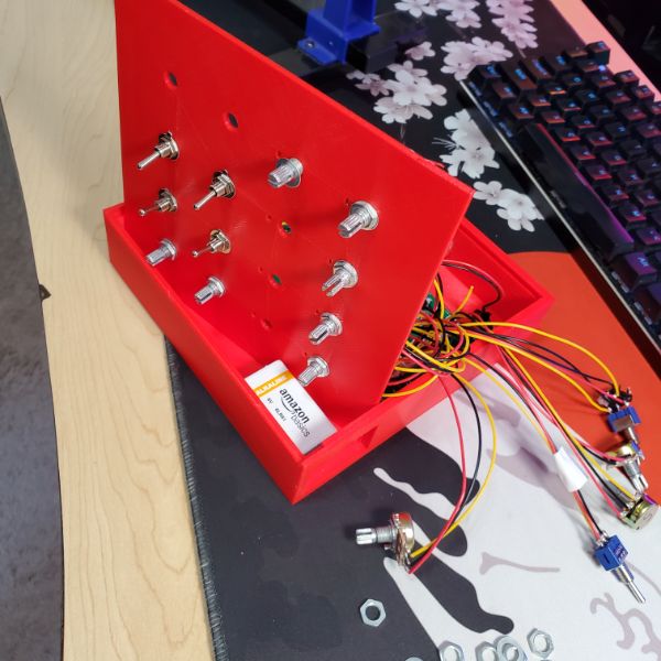
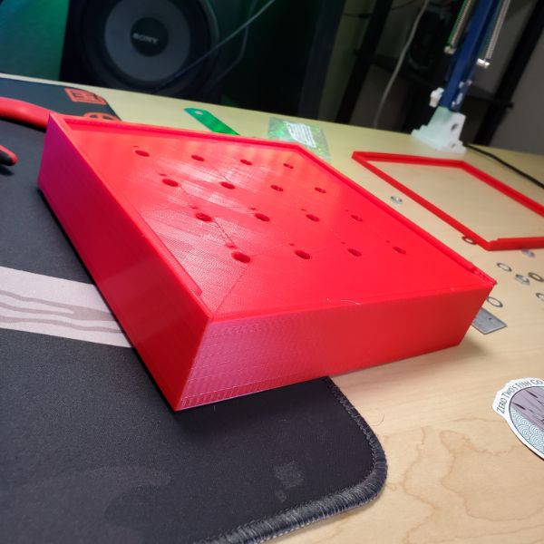
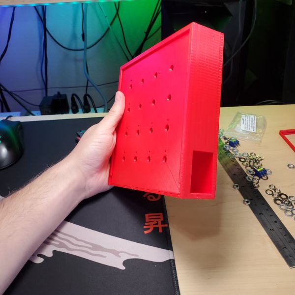
I don’t think the housing should be any more than 5cm deep in total. I layed out 10 pots and 6 switches and I was able to get them all to fit cleanly on top of a blank PCB, so the dimensions of the housing don’t need to be that much bigger than that of the PCB itself, which is nice because this thing will be pretty compact.
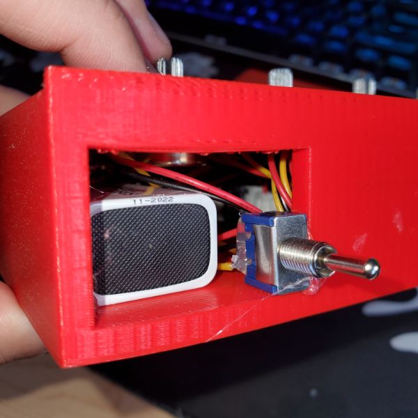
Since I want users to be able to replace the 9V battery without having to expose themselves to the guts of the PCB, I’ll need to design a little 9V chamber in the back of the housing with the pull off cover and everything. That also means I need to buy a 9V battery holder as a part of the parts list for this thing.
with a 5-10cm depth for the housing, the length of the JST connectors I bought won’t be an issue. They’re around 6 inches long.
I still don’t know how I’m going to 3D print a front panel with labels for things. I keep thinking, this would be easier with a Laser Cutter. But I guess since I’m in the market for a new 3D Printer, I could always just get a dual extrusion upgrade and do a multicolor scheme. I have no idea how those things work though.
I’m guessing once everything is designed and assembled, the whole thing will take about 3 hours for picking and soldering parts, cutting leads, soldering pots, and mounting into the front panel. If I wanted to sell these things, I’d have to make it worth my time, so if there was any sort of volume whatsoever I would have to hire someone else to do them for cheap. In terms of parts, it’d be the cost of the PLA, the cost of the parts, maybe $5 max, then the cost of the JST connectors which are like $6 on their own. Then speakers and battery, maybe it’d be around $20-25 in parts for each synth. Discounting labor, I could probably sell these things for $30-60. I wouldn’t feel quite right selling this thing for as much as $60 though. Maybe if I could build more capable, more robust synthesziers, I’d feel comfortable selling something for $150-200 and that would be a more comfortable price point.
I do have books that could make me better at designing synthesizers. The main thing I don’t like about this thing is it’s so high pitched. I would want a synthesizer that could really RUMBLE. Also, how many people even want/need synthesizers? I feel like it’s more in the gadget/nonsense category if you’re not a literal professional. Maybe amateur musicians who want a unique sound
I could sell or just give one to itvlo and matt and I’m sure they would enjoy that.
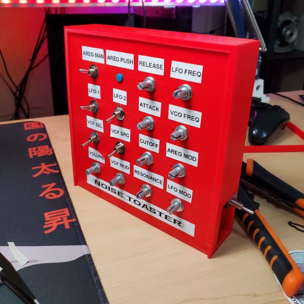
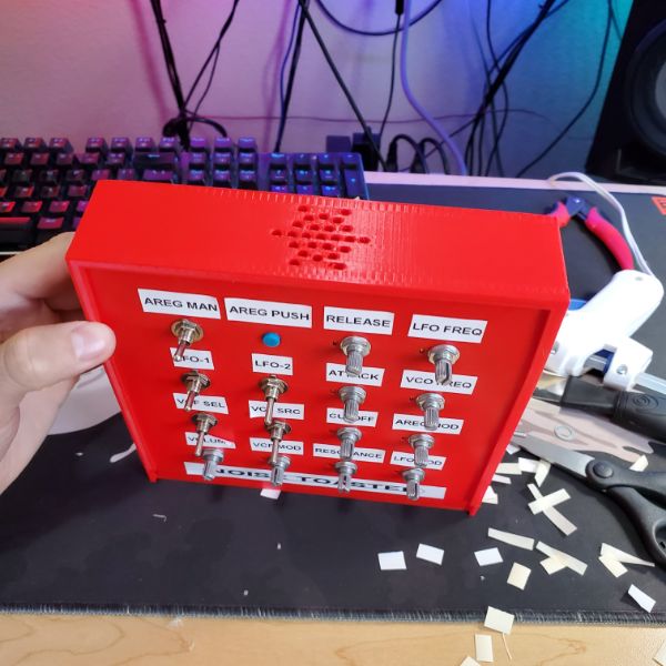
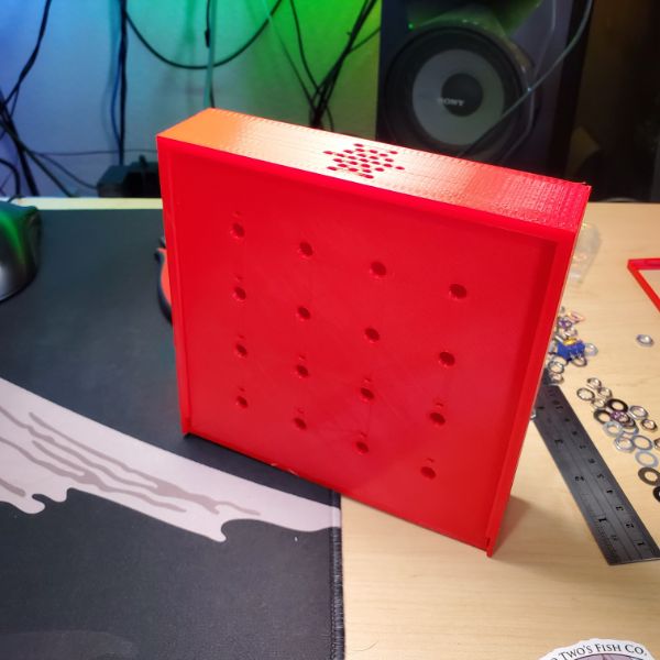
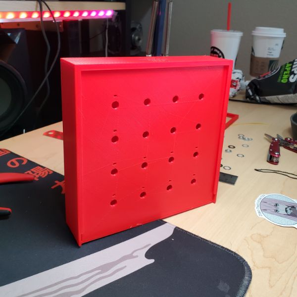
Synth Enclosure
need to print a sheet that has pot
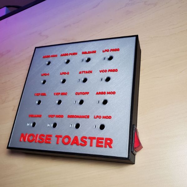
Designed a basic front panel layout for a 150mmx75mm sheet. But the printer doesn’t work anymore so, kms
2022-I
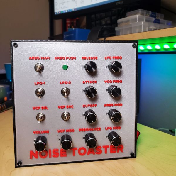
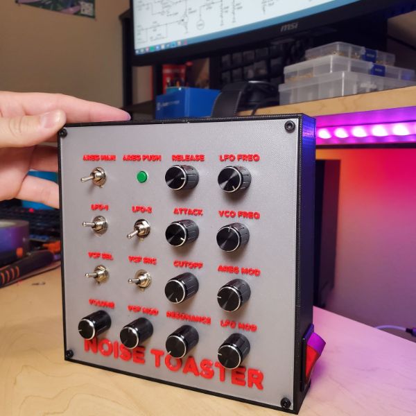
Synth Panel
R2 Print
Took 5h30m and hours of repairing the printer before it came out, but the pots fit into it pretty well. Time to button everything up for the first time and see how it looks
Fit everything into the panel just fine and bolted it down. I had a wire break but it was easy to solder back together.
Hot glued the button into place, and now everything’s where it should be
I was having an issue getting the switches to tight and aligned, so I think I’ll just wait until the body is done so I can get a better grip on it
I need to check for a good power switch, I don’t really want to loot breadbox but I might be inclined to
I’m thinking on the top surface of the case, there will be a hole for the power switch, and then a speaker perforation. Then the speaker can just go into the top and that’s where the sound will come out
The back will need a removable slot for a 9V battery
SYNTH PANEL R2 LAYOUT
F
X
8
0
B
C
7
1
E
D
5
2
9
6
4
3
Horizontally Mirrored Layout
0
8
X
F
1
7
C
B
2
5
D
E
3
4
6
9
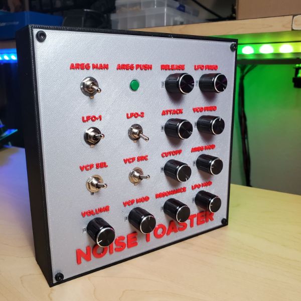
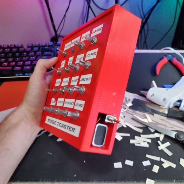
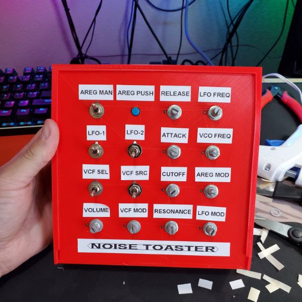
SYNTH PANEL REFDES TABLE
Panel Label
REFDES
Code
LFO FREQ
RV4
0
VCO FREQ
RV1
1
AREG MOD
RV3
2
LFO MOD
RV2
3
RESONANCE
RV9
4
CUTOFF
RV6
5
VCF MOD
RV5
6
ATTACK
RV7
7
RELEASE
RV8
8
POWER
SW1
A
LFO-1
SW3
B
LFO-2
SW4
C
VCF SRC
SW6
D
VCF SEL
SW5
E
AREG MAN
SW7
F
AREG PUSH
SW8A
X
AREG SEL
SW2
N/A
Notes
I printed out the old synth panel design I came up with previously.
The 7mm and 6mm holes I put for the knobs and switches respectively don’t have any functional difference. You can tell visually if you look closely, but both threads fit into both holes so what’s the point.
I can already tell that the panel surface needs to be a lot bigger though, otherwise this thing will be painfully cramped, and end up being less convenient to use anyway
Labeling all the pots, they screw in just fine
Turns out the pots have this little orientation tab that I have to account for. That’s kind of a pain and increases the complexity of the panel design by a lot
I’ll have to create a rectangular recesssion offset for each pot
switches bolt on just perfect
Turns out the underwater effect is cutoff freq
My headass forgot to model a hole for the LFO freq adjust, so now i REALLY have to redesign this thing
Looks like I constrained both circles to 7mm. So I’m just tripping on the visual difference
Either way, both pots and knobs seem to fit just fine if I bypass the metal tab by screwing on a second washer before inserting the knob. That means two washers per pot. Is it worth it? Probably. I can see those tabs becoming a headache on their own pretty quickly. I’ll still give them a quick try though
Since I have 17 UI ports, I’m thinking of putting the power port in the top side of the box and not in the panel, and then doing a 4×4 square grid for the other 16 ports.
I mapped them out on a paper with a layout
I’m thinking a 16cm square, so that there can be 40mm spacing between the center point of each UI node
This also gives me room for the 33-38mm x 12mm labels that the label maker produces. That way I can use the label maker instead of trying to
3d print text
write on it
laser etch?
The primary drawback of the label maker (other than being plain black and white) is the fact that I have to trim the edges off. I can use the straight cut, but the labels generally aren’t long enough to do that twice with a firm hold on the paper. The other option is to use scissors
the other final option is to use the exacto knife and pray
It’s not that big of a deal though, since the labels are literally disposable and I can print more at my leasure
I’ve mapped all the switches and knobs to alphanumeric indicators, and I’ll map those to the pcb refdes as well
Found an issue, there’s a switch that turns off AREG modulation in the VCO. It also didn’t make it into my front panel sketch. I was suspicious it didn’t do anything, but I didn’t confirm that its very slight effect is present until after I soldered it together.
I also confirmed that these 2xON switches contact on the opposite of the wires they’re leaning towards
meaning, if the switch is leaning to the RIGHT NC lead, the contact is touching the LEFT NC lead, with a hinge in the middle of the switch.
I learned this by soldering together all 3 pins of a JST connector -.-
FreeCAD Note:
When carving a shape into even segments, make sure the overlaid dividing lines are construction lines. Otherwise, the definition of the total shape’s outline will get confused and it won’t pad right
2022-J
Noise Toaster
Multicolor Embedded Lettering in FreeCAD->PrusaSlicer
Redesign Synth Case
Timelapse Video – Soldering together second Synth
2022-KL
Noise Toaster
New Body Design
Mounting Holes
The length of an M3 bolt refers to the length of the shaft, not the absolute length of the piece
M3
Shaft
2.95mm
Hex Nut
5.55mm Hex OD
2.6mm Depth
Bolt Head
5.60mm Circ OD
3.15mm Depth
Previous case has a depth of 40mm inclusive
Designing around a 40mm M3 bolt that runs through the entire body of the print
Power Switch
Speaker
Front Panel Design
Front Panel should now rest on top of a lip from a slightly smaller square
The front panel dimensions are 160x160mm
2.5mm lip on all sides means an internal dimension of
155x155mm
Which is attached to a
Parts Ordering
Casing
Carve a hole for the switch dimensions
Design a slide panel that slots into the corner of two walls for the 9V battery
Use the 9V battery holder, extend it to match the length of the battery, and give it a bottom so the battery rests flush in place
Leave the battery head facing out of the casing with enough room for the connector, and enough room for the slide
Test notched slides until you get a good method for them
Power Switch Measurement
rectangular hole inside a 2.5mm thick slab
Measured Dimensions:
26.94mm
Snap Tabs: ~1.4mm
21.30mm
Test Dimensions
29
22
29×22
5mm buffer on all sides
39×32 print area
Too Small
Final Dimensions
41x32mm print area
31x22mm switch gap
Slide Panel Tests
Vertical Printed
2.5 thickness slide
2.5 wide gap
doesn’t fit, spreads the frame
2.75
fits perfectly. pretty satisfying, but there’s not enough friction/grip. the slide can shift around in place
2.625
This is the compromise. It still slides with ease but there’s enough friction, and it doesn’t spread the frame
Add ONE EIGHTH of a millimeter for slides
Horizontal Printed
I have to rerun these tests because the overhang creates issues
2.625
isn’t enough
2.75
Front Panel Slide Rails
Front Panel Dimensions
160mm Across
160mm Deep
2.5mm Thick
Slide Rail Dimensions
165mm x 165mm
7.5mm tall with a 2.625 tall notched vertically centered, cutting in 2.5/5mm deep
Front Panel M3 Bolt Check
Measurements
M3 Bolt OD
5.38mm
Hexagon
>
5.55m Hexagon Diameter
M3 Bolt ID
~2.6-2.75 mm?
Check Spec
Shaft/Thread Diameter
Consistently measures around
2.93, 2.94mm
Consistent with M3 (3mm)
Will make a snug shaft of 2.90mm
Works, but inconveniently snug. Try 2.95
Bolt Head Height
3.04mm
>
3.15mm
Bolt Head OD
5.45mm
>
5.60mm (larger than hex)
M3
Shaft
2.95mm
Hex Nut
5.55mm Hex OD
6.41mm Hex OD
corner to corner
2.6mm Depth
Bolt Head
5.60mm Circ OD
midpoint to midpoint
3.15mm Depth
Front Panel Pocket Depth
Front Panel is only 2.5mm thick
I can print a small 2.5mm slab and have four pocketed corners of varying depths to see which works best
0.5
1.0
1.5
2.0
Those are really the only options
There might be an optimal of 1.25, so I’ll do that in the middle too
1.25 is the move
Or really it would be better to just do a strip instead
Noise Toaster1
Design New Case
Assemble New Board
Record Video