
12/5/2022 – 12/18/2022
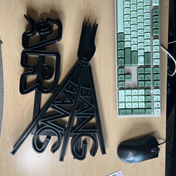
Summary: Been grinding away at the signs, and also reading AoE where I can. Started annotating chapter 2 and reading chapter 3. Also started breaking down Monty Choy’s question list. It’s actually a really good overview of the entire field.
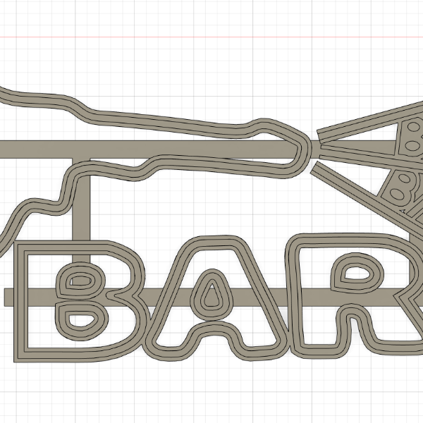
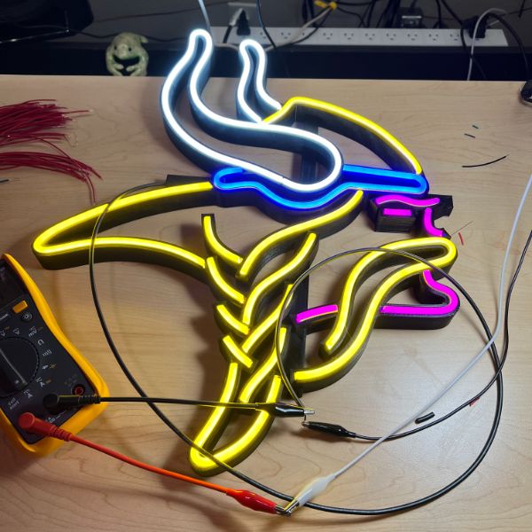
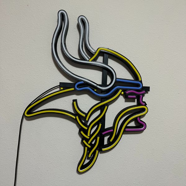
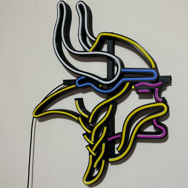
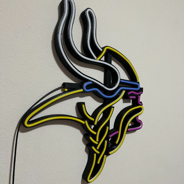
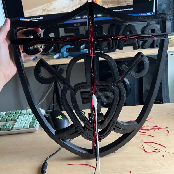
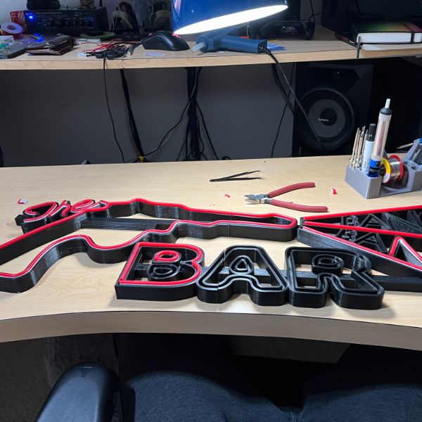
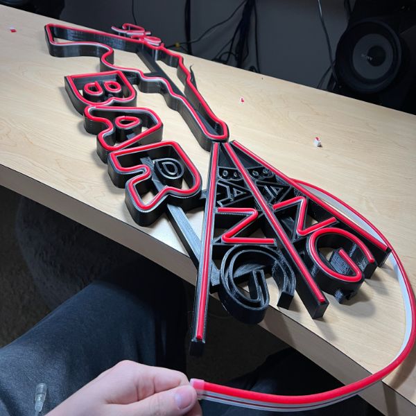
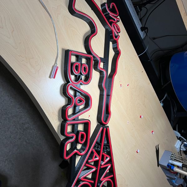
Every sign has had at least one small design defect somewhere that I don’t catch until after print, sometimes not even until wiring. Which means there’s a flaw in my process and I probably need to start making checklists for these things. Reviewing the Ramona Flowers one I restructured the whole design process, but even after doing that I still look at it and come up with better and more efficient ways to do this. All in all, it’s turning into one of those things that just takes time and iterative practice to get it locked down. Also, the Ramona Flowers revealed two dead red pixels after I buttoned everything up and it made me want to pull out my hair zzzzzz. Will probably end up starting from scratch a third time on that one. I can’t send something out at that quality level when I’ve improved the ones after it so much already.
It’s also been challenge stretching my skills and my model of the process as people ask for custom orders like RGB and blinking and whatever else. My plan at this point is to take notes on what could’ve been better about each sign as I ship it for this initial batch, put all that info together and rewrite the SOP for the 3rd time, this time with some QC checklists before print, etc. Then open the store page and raise the prices.
One big thing I need to get locked down is having a realistic estimate for how long I should expect the strips to be. Something I figured out just a few days ago is that the strips have the flexible PCB against one wall of the silicone, it’s not centered. This is obvious but the implication is that the strip is actually longer or shorter around curves depending on whether the PCB is hugging the wall or not. The silicone is stretchy, but not that stretchy and you wouldn’t expect it to make a difference but sometimes it can account for a 1-2cm difference depending on which side the PCB is on. Blew my mind when I caught onto it.
So the three factors really holding back the level of precision I’m looking for on these signs at the moment are 1. estimating strip length design side 2. accounting for chiral strip length changes 3. mapping valid length/cut ranges for the strips. Beyond that, the rest is just design efficiency and double checking at this point. The last big design breakthrough I made was realizing I can use the path spline to create offset lines and easily make really intense curves without having to deal with sweep self-intersection.
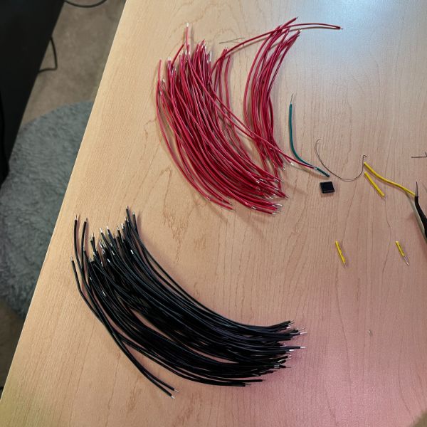
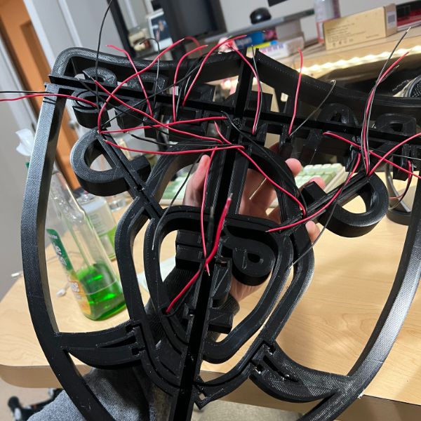
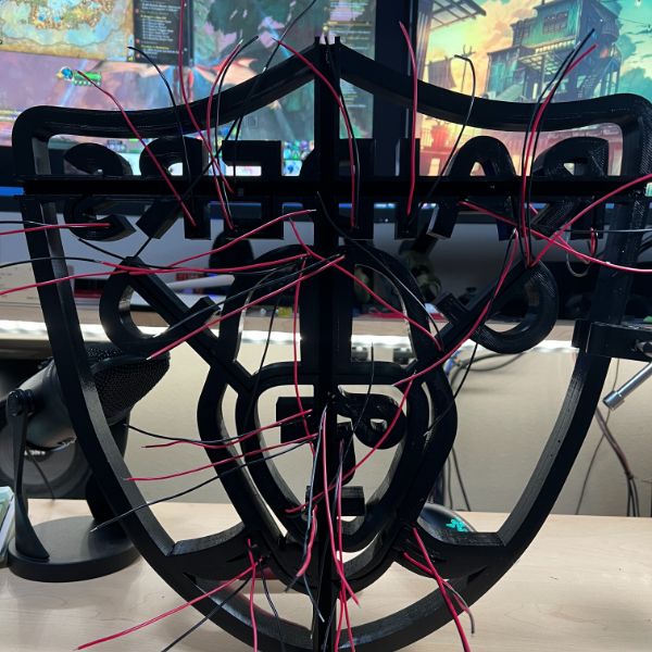
The 2mm wire routing slits are also proving just a smidge too small a lot of the time and actually resulted in a pad break a few days ago, so they should probably be upped to 2.5mm or somewhere in between. I also started cutting 6″ lengths of wire in bulk before starting a sign. It takes an hour or so but saves a lot of hassle down the line when it’s time to actually wire a sign. In addition to that I bought a precision hot glue gun to prevent pad breaks, and it seems to be helping. I’ve also gotten decent at using the wedge tip of the soldering iron to make edits to the frame after print. But that’s a last resort thing and I don’t like doing it.
At this point, all the orders I needed to get done by Christmas are done and I’ve only got 3 more to do after New Years once I’m back home


Yak
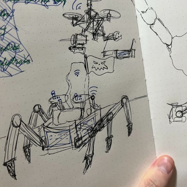
Ideas
12/5/2022 – 12/18/2022
Monty Choy
Basic Circuits
Passive Components
Resistors
Capacitors
Inductors
Physics/Chemistry
Semiconductor Devices
Device Physics
Diodes
BJTs
MOSFETs
Analog Circuits/Electronics
Random Circuit
CMOS
Amplifiers
Opamps
Filters
PLL
Power Electronics
Power Electronics
General Power Supply
Power Supply Topologies
Efficiency
Power Architecture
Buck Converters
Duty Cycle/Output Voltage
Circuit Analysis
Power Bridge
Efficiency, Ripple, and Switching Frequency
Voltage/Current Sensing
PFM Operation
Multiphase Buck Converters
Controls/Stability
Designing Buck Converters
Debugging, Validating, and Characterizing Buck Converters
Boost Converters
Low-Dropout Regulators (LDOs)
Charge Pumps
Batteries
Lithium Polymer (LiPo)
Monitoring
Chargin/Discharging
Safety
Inductive Loads
Inductive Loads
Characterization/Behavior
Brushed DC Motors
Brushes
Brushless DC Motors (BLDC)
Electronic Speed Controllers (ESCs)
Stepper Motors
Servo Motors
Safety and Monitoring
Speed/Position
Single-Phase Inductive Drives
Half/H-Bridge
Control from Embedded Device
Current Sensing
Current Sensing
Sense Resistor
Current Sense Amplifiers
Current/Voltage Protection
Printed Circuit Boards (PCBs)
Printed Circuit Boards
Layers and Materials
Stackup
Design/Layout/Routing
Grounding
Decoupling/Bypass Capacitors
High-Speed Signals
Differential Pairs
Transmission Line Effects
Board-Level Termination
High-Current Layout/Routing
Power Supply Layout/Routing
Power Supply-Level Layout and Placement
Component-Level Layout/Routing
Sense Resistor Layout/Routing
Noise, Interference, and Coupling
EMI Shields
Vias
Testing PCBs and Design for Excellence (DFX)
PCB Fabrication
Manufacturing and Assembly
Automated Testing
Design for Manufacturing (DFM)
Design for Testing (DFT)
Test Points
Debugging and Making Measurements on PCBs
Reworking PCBs
Electrical Computer-Aided Design (ECAD) Software
Packaging
IC Fabrication
Signals
Square Waves
Differential Signaling
Signal Integrity/Power Integrity (SI/PI)
SIgnal Integrity (SI)
Differential Pairs (SI Perspective)
Power Integrity (PI)
Transmission Lines
TL Theory
Ideal vs Real TLs
Embedded Systems
Embedded Systems
Microcontrollers
Communication Buses
I2C
Protocol Layer
Physical Layer
SPI
UART
GPIOs
Design/Implementation
Timers
Interrupts
Peripherals
ADC
DAC
Data Storage and Memory
Debugging Embedded Systems
Operating Systems
Sensors
Sensors
Gyroscope/Accelerometer
Light
Camera
LiDAR
Calibration, Validation, and Testing
Digital Basics
Digital Basics
Digital Electronics
Logic Gates (Digital Perspective)
Digital Logic
VLSI/Computer Architecture
Computer Architecture
GPU
System on Chip (SoC)
Memory
Power/Performance/Thermals
RTL
Assembly
Coding
Coding
Variables
Programming Questions
System Architecture
Measurement
Measurement
DMMs
Scopes
Scope Probes
General Debug, Testing, Validation
Non-Technical
Intro
Behavioral
Technical/Behavioral
AOE
Chapter 2
2.1 – Introduction
Notes
A transistor is an active component
Active components amplify
Defined as: the output signal has more power than the input signal
The transistor is the single most powerful resource for interfacing everything in electronics – ICs, circuits, subcircuit modules, etc.
BJTs came first, before FETs in 1947
Simple comparison:
BJTs
Low noise, accuracy
FETs
Low power, high impedance, high-current switching
Transistors have 3 terminals, EBC
Emitter, Base, Collector
Vc – Voltage from collector to ground
Vce – Voltage from collector to emitter
Vcc – refers to positive power supply voltage, usually on collector side
Vee – negative power supply voltage, usually on emitter side
Vcc and Vee probably won’t change polarities if you start working with PNPs though
Transistors are 3 terminal devices, which means there are two voltages and two currents to juggle
Not 3 currents and voltages, because only 2 are independent. the third one is dependent on the other two
2.1.1 – First transistor model: current amplifier
BJTs have three terminals
a small current into the base controls a large current through the collector-emitter
comes in npn and pnp variants
NPN Rules (reverse for PNP)
1 – Polarity
Vc must be greater than Ve
2 – Junctions
Base->Emitter and Base->Collector act like diodes
Base->Emitter diode is usually conducting
meaning base is higher than emitter by at least one diode drop
Base->Collector diode is usually reverse biased
current can’t flow into the base from either E or C
Control current flows into B and out through E
3 – Maximum Ratings
All transistors have max values for
Ic – current flowing through collector-emitter
Ib – current flowing into base
Vce – voltage across collector-emitter
exceed them and it breaks
Other limits worth noting
Max power – Ic * Vce
Max Vbe
4 – Current Amplifier
If 1-3 are followed
Ic is proportional to Ib
Ic = B*Ib
B is Beta which is h_fe
“h parameter transistor model” is no longer popular
PNP Rules
1 – Polarity
Ve must be greater than Vc
2 – Junctions
Emitter->Base is diode
Collector-> Base is diode
Control current flows into E and out through B
3 – Maximum Ratings
4 – Current Amplifier
Beta is a shitty parameter that should not be relied on
Beta varies with
collector current
collector-emitter voltage
temperature
the base-emitter voltage Vbe acting like a diode (rule 2) means you can’t put arbitrary voltages across Vbe
if you put more than one diode drop (0.6-0.8V)
immense currents will flow and probably kill your transistor
For an operating transistor (NPN)
Vb = Ve + 0.6V
For an operating transistor (PNP)
Vb = Ve – 0.6V
Don’t think of collector current in terms of the base-collector diode
the voltages are usually applied in the wrong direction
collector higher than base, diode is Base->Collector
Collector current varies little with Collector voltage
in diode conduction, current rises quickly with increasing voltage – this is not the case with the base-collector junction
to summarize these two diodes
the base->collector one is just there to let you know that collector current can’t go into the base
the base->emitter one is there to restrict Vbe to one diode drop
2.2 – Some basic transistor circuits
2.2.1 – Transistor Switch
If you give the base say 10mA and the beta is 100, then you would expect 1000mA to go through the collector
but that doesn’t always happen
since the emitter is usually connected to ground, Vce is just Vc,
and since the load the transistor (NPN) is powering is usually placed between the collector and the Vcc positive power supply,
the voltage across the load determines how much current will flow through the load and the transistor (collector current)
In order to increase the collector current, Vc decreases
So for LARGE Ic, there’s usually a SMALL Vce
and similarly, for a SMALL Ic, there’s usually a LARGE Vce
Meaning there wouldn’t be a large voltage drop across the load, so the transistor eats up the rest of the voltage to ground by holding it up at the collector
If a transistor needs to provide it’s maximum amount of current, it’s said to enter a state of “SATURATION” and Vc goes as close to ground as it can
This is usually about 0.05 – 0.2V
when you send wayyy too much current into the base, that’s called overdriving
when you overdrive the transistor, it doesn’t blow itself out trying to keep up
the transistor would’ve saturated at 1mA (Beta of 100, Ic = 100mA)
Everything more than 1mA going into the base is superfluous
Note – beta goes down when Vcb is low
Note – add pullup or pulldown resistors
pulldown resistors for NPN – to connect the base with a path to ground when unpowered. this keeps Vbe at zero and prevents conduction
pullup resistors for PNP – to connect the base with a path to Vcc when unpowered. this keeps Vbe at zero and prevents conduction (in this case E is connected to the power supply rails as well)
NPN Base gets switched to positive supply, and some of the current into the base gets routed through the pulldown resistor,
PNP Base gets switched to ground, and some of the current coming out of the base
3 Design tips for Transistor Switches (BJT)
1. Choose the base resistor conservatively to get plenty of excess base current, especially when driving lamps
lamps draw more current when they’re cold
2. If the load is AC or inductive and liable to swing below ground, place a diode Load->Collector in series with the load to prevent the Base->Collector diode from conducting
3. If the load is inductive, protect the transistor with a diode in parallel to the load pointing to Vcc (Parallel Collector->Vcc)
this is called inductive kickback (flyback?)
5 Reasons why transistor switching is superior to mechanical switching
1. transistor switches can be driven electrically from another circuit (interfacing), like from a computer bit
2. transistor switches can enable extremely fast switching speeds (microseconds)
3. you can switch many circuits with a single signal
4. mechanical switches have wear and tear, and they bounce
contactor bouncing
5. remote, cold switching means cables don’t have signals, just DC running through them. this means less signal travel, crosstalk, signal degradation, etc.
Transistor Man
Transistor man’s perpetual task in life is to try and keep Ic = B*Ib by turning a little knob
The knob controls a resistor and he can slide it from
zero ohms, short circuit, saturation, zero Vce
infinite ohms, open circuit, cutoff, max Vce
Transistor three states
Cutoff – High voltage on Vce, No Collector current
Active Region – Some voltage on Vce, Some Collector Current
Saturation – a few tenths of a volt Vce, Max Collector Current
2.2.2 – Switching circuit examples
Notes
A transistor switch is a Nonlinear circuit: the output is not proportional to the input.
After a certain threshold is reached, it abruptly switches from one state to another
The output is not continuous, proportional to the input
In transistor switches, the transistor does not use the active region, it is either in saturation or cutoff
linear circuits contain amplifiers, current sources, integrators, etc and offer more interesting challenges and room for creativity
note, for this section, switch ON means Saturation mode
Switch OFF means cutoff mode
A – LED Driver
Most LEDs are just diodes that start conducting around 1.5-3.5V
A 10-20mA LED will burn your eyes
Because of the Steep IV curve, 5V across an LED will blow it out.
In the basic LED Driver circuit, we use the base resistor conservatively to make sure there’s more than enough base current to ensure the transistor is in saturation
When selecting the collector resistor, we pick a value to set the operating current
Since the LED’s voltage drop is known, and the power supply voltage is known, and we know that the transistor only has a few tenths of a volt across it in saturation (which we can round to zero), it’s easy to pick a resistance for the remaining voltage to set an operating current for the LED
There are ways to devise circuits that provide an accurate output current, independent of what the load is doing (current source configuration)
B – Variations on a theme
Notice the NPN BJT switch circuit connects the load to the positive rail, and the transistor’s switching action makes and breaks a connection to ground.
What if you wanted to connect the load to ground, and use the transistor to make or break a connection to the positive rail?
You would use a PNP switch instead
Why can’t you just put the load on the emitter of the NPN?
Remember that when the switch is ON and the transistor is in saturation, there’s a 1Diode drop between the base and the emitter, and the drop between collector and emitter is nearly zero.
the range of voltage drop across the load is then reduced by 1Diode drop, rather than being capable of full swing (Vcc to Zero)
there are subtler effects concerning the resistance between the emitter and ground not discussed yet, as well an effect where the base and collector current add at the emitter
So the circuit would work, but it’s much better practice to keep the load strapped to positive rails for NPN, and strapped to ground for PNP
PNP switch circuit
the emitter has an arrow pointing INTO the transistor, it’s on the upper part of the symbol, and the emitter is connected directly to positive rail
the collector is on bottom and connects to the load and then to ground
some things that are different
the combined emitter current enters the transistor from the positive supply and forks
the base current LEAVES through the base and then the remainder goes out through the collector. This is what powers the load.
This also means that current won’t be able to flow out through the base until the input signal to the base goes LOW.
That means the PNP switch is an ACTIVE LOW circuit.
When the voltage applied to the base is high (VCC) there’s no voltage difference between Base and Emitter
When it goes low (ground on the resistor), the base will drop 1Diode from the emitter/Vcc, and the rest of the voltage will drop to ground through the resistor.
barebones PNP switch circuits like this can be awkward to work with because the OFF state requires the base be held all the way up at Vcc, which could be 10, 12, 15, 20 Volts. Most control voltages in computers and microcontrollers are either 3V or 5V (called logic level) and so they wouldn’t be able to control a PNP switch as easily as an equivalent NPN switch
In order to get a PNP switch to work with a 3V control voltage, just attach to the base of the PNP switch, another NPN switch.
The NPN switch will receive the 3V, turn on, and when it turns on, it’ll create the high voltage at the base of the PNP switch that’s required to turn the PNP off
Figure 2.10B
R3, 1k, connects Vcc to the Base of the PNP
When the PNP is on, that 1D drop from E to B means that the B node will be at a voltage of 14.4V
Since that is true, the resistor connecting Vcc to B will have to drop 1D as well, meaning it’s current will be low
The resistor below that can be expected to drop the rest of the voltage before the near zero Vce of the NPN
so the remaining 14.4V’s pass through current can be set by the selection of R2
note that this 14.4V current through R2 is a combination of the current through R1, and the base current of the PNP. Most of it will be coming from the base current of the PNP
When the NPN is cut off, and there’s no path to ground through R2, no current will flow through R2 or R3, and the base of the PNP will be held up at 15V.
Once a 3V control signal is applied to the NPN, the NPN will go into saturation, create the path to ground, and allow the base of the PNP to go low enough to allow itself to also enter saturation.
Note that the switch example circuit had the PNP base switching from 15V to 0V. Realistically, one diode drop away from Vcc is all that’s necessary. So it’s just fine that instead it’s going from 15V to 14.4V.
Once the 1D drop on the PNP’s Vbe is established, it goes into saturation and pushes current through the load by creating a connection to the positive rail.
In this case, there are two determinants for the current through the load
1. the Ic=B*Ib, where the base current of the PNP is set by R2
2. the resistance of the load on Q2
C – Pulse Generator – I
for this circuit, before the input signal goes high, the passive, ambient state of the circuit
the initial condition
check the transistors and figure out what state they’re in during initial conditions
Q1 is OFF, obviously, because the input signal has yet to come
Q2 is ON, because R3 creates a direct path to Vcc for Q2’s base
we also know that because Q2 is in saturation, there is a 1D drop for Q2’s Vbe
since the emitter is grounded, that means that Q2’s base is at 0.6V
with this information, it’s easy to calculate the current going through R3, since we have both the resistance and the voltage across the resistance
what’s more interesting is on the other side of the capacitor. since Q1 is OFF, there’s no path to ground there, meaning the Q1 collector node is at Vcc.
There’s no path for current to flow and so there’s no voltage drop across the resistor.
This means that the capacitor has 5V on the left, and is at 0.6V on the right. The Capacitor has 4.4V across it.
Something is going to change once Q1 receives the input signal and opens a path to ground
Since Q2 is ON, in saturation, and a large current flows through it, R4 is there to limit the current passing through so the transistor doesn’t cook
it’s also there to create an output terminal. without the resistor, Vcc would be directly connected to the collector of Q2. What do you measure then if you want an output voltage? It’s just going to be Vcc
This is why resistors can be interpreted as devices that convert currents into voltages. There was no voltage or voltage drop to measure before the resistor was added, just a current.
what happens when the input goes high?
First, the path to ground opens up, dropping the Q1 collector from Vcc to Ground
This voltage drop means there’s now current flowing through R2
two things are true at this point:
the left side of the capacitor is at 0V
the left side of the capacitor is 4.4V higher than the right
because the voltage across a capacitor cannot change instantaneously, the right side’s voltage moves from 0.6V down to -4.4V.
Now, the base of Q2 is at -4.4V and does not meet the 1D criteria and switches off, from saturation to cutoff
because R3 is still connected to Vcc, and its other terminal is now at 4.4V, there’s a 9.4V drop across it, meaning a lot of current is flowing through R3. It doesn’t have a path to ground through Q2, so it has to go through the capacitor
because a current is flowing into the capacitor, the voltage of the capacitor must change. this is the fundamental law of a capacitor.
In this case, a positive current is flowing into the negative terminal, which nullifies the stored charge in the capacitor, lowering it’s stored voltage, rather than increasing it
since one side is fixed at ground, the discharge effect doesn’t change the voltage of the left side, only the right. As the current from R3 flows in, the voltage at Q2’s base slowly increases from -4.4V up past zero (at which point the capacitor begins storing charge again, but with opposite polarity), until it reaches 0.6V again and turns on Q2.
note that during this time, as the voltage on the right side increases, this charging action will decrease the voltage drop across R3, and so the current will taper off too.
It’s important to note that this charging, if uninterrupted by Q2’s reactivation, would continue charging all the way to 5V. At that point, the left terminal would still be at 0, and the capacitor would have a full 5V across it. The current through R3 would slowly reduce to zero, as R3 would have 5V on both sides.
once Q2 turns on, both transistors are on at this point, and both provide paths to ground on either side of the capacitor.
Also, both terminals of the capacitor are locked in place by the two transistors, meaning no current flows through it any more. It still has a 0.6V charge, but that voltage is not changing
If the voltage isn’t changing, there’s no current. this is the rule of the capacitor.
as for the output behavior of the circuit, it’s either 5V or 0V depending on whether Q2 is on or off. If it’s on, then current flows through Q2 and R4 drops 5V, and the output voltage is zero. If it’s off, then no path to ground is available and there’s no voltage drop across R4, so the output voltage is 5
Q2 ON
Vo = 0V
Q2 OFF
Vo = 5V
So the general characteristic is that it creates a pulse of fixed length after receiving one high input swing. in this most basic case, the output is a switch that gets turned up high and remains high indefinitely.
how is pulse length determined?
right away, we already know that the pulse gets cut off by Q2 re-entering saturation once the right side of the capacitor moves reaches 0.6V.
We already established earlier that the left side gets held at ground, so the charging action is taking place on the right side, where current moved through R3 into the capacitor.
This means the time constant for this charging action it t=R3*C
Recall that the charging action starts at -4.4V and would continue charging all the way to 5V if uninterrupted by Q2’s resaturation
So, the duration of the pulse is just the time constant times the time travel factor 5/9.4V (0.53) -> [-ln(1-0.53)]
D – Pulse Generator – II
first, a major draw back of this circuit is that the output pulse has a predetermined length, but it can get cut short if the input goes low again before it’s finished.
the output pulse should be the same regardless of how long the input is high
once we fix this, this means that this pulse generator only triggers on the RISING EDGE
so first, in the cut-short scenario, we send a brief input signal, and q1 momentarily activates, shorting the left node to ground, swinging the right side into the negative voltages, and the capacitor starts charging up towards +5V
before it can charge all the way up to activate Q2 again, the input signal turns off and the capacitor charging curve is reset. no dice
What we need is to keep the left node grounded until the capacitor finishes it’s work
1. what circuit structure can we use to create a conditional path to ground?
an NPN transistor switch
2. what signal in this circuit corresponds to the capacitor indicating it’s done charging?
the output signal of the circuit
it goes high when Q2 is off (while the capacitor is charging)
it goes low as soon as the capacitor is done charging
so what we can do here is take the output signal and plug it into the base of an additional transistor.
Now, when Q2 is Off, the output is HIGH, and so Q3 will be ON
we want the path to ground to be valid while the capacitor is charging (output is high) and so NPN is the right choice here
So we just connect the Q1 collector node to the collector of this new Q3, and now whenever the output voltage is HIGH, this node will be held to ground, regardless of whatever dancing is happening at the input
it needs a little elaboration though. we want to add a resistor between the output node and the base of q3 so there can be a voltage drop. we want the output voltage to stay at 0 and 5 volts, while the base stays at 0 and 0.6V.
without a resistor, they’ll be the same, we want them different, so we split them up
next, we need to look at the currents flowing through these resistors so we can pick the right resistance value to keep everything in line.
we need to consider what states these two transistors might be in to understand what currents are going to flow where and when and how much etc etc.
first, note that we put q3 here to provide a path to ground while the capacitor charges
if the capacitor is charging, that means q2 is OFF and the output is HIGH
if q2 is ON, the output is LOW and will essentially be grounded
This means the base voltage going into Q3 will not be above 1D and q3 remains off
all this means Q2 and Q3 are mutually exclusive
if the output is LOW, we don’t need to consider the currents through the q3 B resistor, because there is none
if the output is high, there will be some current flow through R4 and then through R5 (it will never split and go through Q2 (mutually exclusive)) and then into Q3’s base and out through it’s emitter to ground
so essentially, we have a voltage divider placed between 0.6V and 5V (4.4V to divide).
Some current is going to drain through the q3 base resistor and out through its base when q3 is on. this is unavoidable and will reduce the output’s voltage from 5 (no current flowing) to just under 5 (some current
We want the voltage at the output as high as possible, so we want the second resistor to have a much higher value.
in this case, 20k vs the 1k should be fine
now we can calculate that 4.4V divided into 21k makes about 200uA, and the voltage at the output on HIGH will be around 4.8V vs the original 5V. good enough for us
We could increase this 20k resistance, but then the total current would go down, and that would require a higher Beta value on Q3 for the same performance.
We don’t want to design circuits that are dependent on a specific value of beta, and the lower the minimum necessary the better, since most are around 100.
to check the beta, let’s see how much current needs to flow through the Q3 collector, and how much current is available going into the base
collector sees 5V across 1k, so 5mA or 5000uA
base sees 200uA,
Since Ic = B*Ib, we can calculate that Beta needs to be at least 25 for this circuit
so as long as we can find a transistor with at least 25 Beta and our 5V output is acceptable to 4.8V this is a fine addition to the original design
With the addition of this extra transistor switch creating a new conditional path to ground, the output pulse length is now completely independent of the input pulse length, such that this is now a RISING EDGE TRIGGERED PULSE GENERATOR
E – Pulse Generator – III
There’s still one more deficiency to this circuit to fix
As the capacitor charges up until 0.6V is reached and Q2 turns on the 100us time constant means it will leisurely cross that threshold and slowly activate Q2. meaning the output voltage will not abruptly drop from 5V to 0V, but will decay gradually to the new voltage level
One way of fixing this is to add a schmitt trigger to the output
a schmitt trigger is a circuit that uses hysteresis or regenerative action to turn a slow moving waveform into an abrupt transition
a schmitt trigger consists of two transistors whose emitters are connected to ground through a shared small resistor
then, the secondary transistor’s base is connected to the first transistor’s collector, making it so when q1 turns off and breaks the path to ground, q2 turns on.
both transistors have resistors between collector and Vcc to limit current, obviously.
first, the fact that the shared emitter resistance is small means that both q1 and q2’s base will still be around 0.6V above ground (slightly more, but still not more than say, 1V)
circuit passive state, before input goes high
Q1 is off, Q2 is on, Output is 0V
Q1 is on, Q2 is off, Output is 5V
q1 OFF, q2 ON – mutually exclusive
because q2 is ON, we know that current is flowing through the collector and through the base, combining inside the transistor, and leaving through the emitter.
in this case though, there is a tremendous excess of base current passing through, and a fully saturated collector current.
We know that the voltage at the collector in saturation is near zero, so we can assume a full 5V across the 1k resistor (ignoring the negligible voltage drop on the small shared emitter resistor)
meaning 5mA through the collector
But similarly, we also have 5V dropping to 0.6V on its way to the base. So 4.4V/1k means 4.4mA going through the base and combining to make 9.4mA total going through the small resistor
Note the logic behind the circuit math here is rough and excludes the small emitter resistor until the end
the proper way to do the math here is to use a system of two equations for two unknown variables
Variables
Formulas
Ie
Ie = Ib + Ic
Ve
Ve = 20*Ie
from there, it can be found that Ie = 9.4mA and Ve = 180mV
now because Ve = 180mV, the required base voltage to turn on Q1 is going to be 1D above that, meaning the ON threshold is at 780mV rather than 600mV.
Once that 780mV threshold is reached, the next state of the circuit precipitates quickly.
First, Q1 begins conducting, grounding the collector of q1. This also grounds the base of Q2. So they switch states at the exact same time.
Then, because Q2 is no longer conducting, both the emitter and base currents disappear and are replaced by the singular collector current of Q1 (5mA)
because the current going through the shared emitter resistor suddenly dropped from 9.4mA to 5mA, Ve also drops from 180mV to 100mV
Finally, because the Ve has dropped, the new threshold value moves from 780mV to 700mV.
Because this all happens at the same time, the input voltage is still at 780mV but because the threshold has suddenly decreased to 700mV, the Q1 suddenly becomes fully ON and nearly instantly switches from cutoff to saturation.
The useful property of this circuit is that the moment the ON threshold is reached, the ON threshold suddenly drops such that the transistor has no choice but to instantly saturate. Even the longest of time constants and most leisurely of waveforms will be converted into an abrupt transition
Q1 is on, Q2 is off. The threshold to drop Q1 into the off state is for the input voltage to drop below 700mV.
Similarly, the whole process repeats in reverse for the input FALLING EDGE
The moment the input drops below 700mV:
Q1 stops conducting
the q1e current stops
the q1c/q2b node rises in voltage
the q2b+q2c current emerges
the voltage at Ve goes up
And so the moment the input falls enough to cross the threshold, the threshold is instantly moved back up to 780mV, placing the Q1 base voltage well below the minimum conduction point, and instantly cutting it off, rather than slowly moving out of saturation.
By moving the thresholds in this way, the circuit becomes “sticky” and has “memory” because it “knows” whether it’s on the way up or on the way down
It behaves differently when it’s up or down. the parameters change
this memory effect or state dependence is called hysteresis
An approximate relationship to determine the distance between the two thresholds is
dV ~~= R_e / R_c * Vcc
where the Rc for both q1 and q2 are the same
The RISING threshold is 780mV
The FALLING threshold is 700mV
So they look like this on a number line
<—| [gap] |—->
If they didn’t have the gap, it wouldn’t work. for example if rising was 700 and falling was 780, you’d cross one threshold and then instantly cross the other, it just doesn’t make sense, move on. accept the gap
2.2.3 – Emitter follower
Notes
The previous circuits were switches, with very nonlinear behavior
meaning, sudden transitions, abrupt on/off states, etc.
The next few circuits are linear, which means the output will be proportional to the input*
*within the intended circuit operating range
an emitter follower is a bjt circuit that follows the emitter
meaning, the emitter is the output
before the output was the collector
now its the emitter
emitter follower
follow the emitter
anyway
also notice that the emitter follower does not have a collector resistor
but it DOES have an emitter resistor
whole thing is flipped around
this circuit is not a switch anymore
because it doesn’t have the collector resistor and emitter straight to ground
it’s an emitter follower
it has an emitter resistor
the emitter can be the output voltage *because* there’s a resistor between the emitter and ground
There is no collector resistor in an emitter follower.
the output voltage is just the voltage at the emitter
and we know that the base voltage is 1D higher than the emitter when the transistor is on
assuming the transistor is on (otherwise this circuit is unpowered and not doing anything)
then we know that the output voltage will be 1D lower than the input voltage or -0.6
Now this seems stupid and this circuit is a waste of space
except remember that we are now dealing with a linear circuit
not a digital/switchy/nonlinear circuit
analog, continuous fluctuations in the waveform of the input are to be expected
we’re now dealing with signals because we’re in linear territory
and so we might have a 2V sinewave that is fluctuating all around
but when we pass that 2V sinewave through an emitter follower, it becomes a 1.4V sinewave
impressive
What happens if the input of the sinewave drops below 1D and the transistor turns off?
Well, the transistor just turns off and nothing passes through
which means that not all of the wave gets passed through
in fact, more than half of the wave doesn’t get passed through.
because a 2V sinewave goes from +2 to -2 and if it stops conducting at +0.6 then everything from -2 to +0.6 (2.6V/4V total) will just be a flatline on the output
this circuit appears more useless by the minute
INPUT AND OUTPUT IMPEDANCE – SOURCES AND LOADS
to understand the value of the emitter follower you need to understand input and output impedance
in electronic circuits, you’re always plugging something in to something else
that is, there are circuit MODULES that are known to have INPUTS and OUTPUTS
MODULES have INPUT and OUTPUT TERMINALS – 2 SETS – BOTH SETS
SOURCES have OUTPUT TERMINALS
LOADS have INPUT TERMINALS
when you have some source, like a power supply, and you connect a motor to it, the power supply becomes LOADED
That is, there is some internal circuitry in the power supply that produces some output voltage, and then there are two TERMINALS for something to connect to that power supply and become part of the circuit
we earlier considered a 10V, 0.1A lamp. Meaning for the lamp to operate properly, it needs 10V dropped across it and 0.1A going through it
We can multiply these numbers together and see that the lamp demands 1W of power
power seems like the right way to analyze how much energy a source is sending out to it’s loads and devices but that’s not how we do it and it’s not as useful
Instead we divide the 10V/0.1A as in R=V/I and turn the lamp into a resistor of 100R.
Now we know that the circuit will behave more or less identically if we replace the lamp with a 100R resistor.
thus, the lamp is considered to be a 100R LOAD onto the circuit
Now, we can estimate what Loads are appropriate for what sources through the analysis of input and output impedance
First, if you’re looking IN to a module, then you are working with its INPUT TERMINALS which means we treat it as a LOAD.
Loads don’t output, they input. They don’t give, they take. Inputs take things. Outputs give things
If you’re looking OUT of a module, then you are working with its OUTPUT TERMINALS, which means we treat it as a source.
INPUT IMPEDANCE = LOAD IMPEDANCE = INPUT TERMINALS
OUTPUT IMPEDANCE = SOURCE IMPEDANCE = OUTPUT TERMINALS
Now in the absolute most abstract sense, when we plug the most abstract source into the most abstract load, we always get a voltage divider.
That is, there’s a voltage source, then the internal source resistance, then the load resistance.
If you want your signal to actually show up across the input terminals of whatever device you’re feeding it to, you need most of the voltage drop to occur on the second resistor, the load resistor.
Another way of saying that is, you want the internal source resistance to be much much lower than the load resistance
Ideally, several orders of magnitude, 2 or 3 is fine
Example, if you have a 10V sinewave source, but the internal resistance and load impedance are both 100R, then only 5V are going to show up in the 100R load.
If you’re expecting 10V and need 10V, you will be sorely disappointed and you will have only yourself to blame for using a source with such high output impedance.
We like small output impedance. We like big input impedance
If you need to remember this, just draw the electronics triangle |>
If you want to go through it, you pass a big wall on the way in, and pass a tiny tiny dot on the way out
BIG input impedance (when acting as a load)
small output impedance (when acting as a source)
Better example, you have a 10V sinewave with a 5R output impedance and you connect a load with 500R input impedance
now, you get 500/505= 99% of your original signal voltage across the load. much better. raise. promotion. brilliant work.
A – Impedance of sources and loads
The Emitter follower’s utility comes from the fact that its input impedance is much higher than its output impedance
It’s a good triangle |>
when used as a load, it has a high input impedance and eats up most of the signal, irrespective of most source impedances
when used as a source, it has a low output impedance, and gives most of the signal it’s sending to the load.
This means a very weak signal that’s not pushing a lot of current or power can pass through an emitter follower, trade off 0.6V from its signal, and receive a tremendous current/power gain.
what was once a weak whisper is now a firm voice. Because the signal going into the base is controlling the flow of a larger output current coming from the 10V source.
Maybe it can power a speaker or something now
Voltage gain isn’t everything
Most of the time we want the source to be “stiff” compared to the load
Meaning, regardless of what load we connect, the source remains the same, or about the same
this can only happen if the source impedance is low enough that any load you might connect is still >90% of the combined resistance and thus received most of the voltage signal
It is always nicer if signal levels don’t change when a new load is connected
Also, in cases where the input impedance of the load can vary with it’s received signal level, then the stiff source always providing the same signal strength regardless of input impedance fluctuations will ensure the circuit can “maintain linearity”
output proportional to input – not freak out and start going all over the place
There are two cases where we don’t want Zin >> Zout
1. Current sources
the whole thing flips
a current source is a source in parallel with its source resistor
the load resistor acts as a parallel resistance and the net resistance between the two has to be calculated in parallel instead of in series.
if you’re using a current source then you obviously want to deliver current to something and so if you have two resistors that need to share one current source, you’d want the load to receive as much as possible and the internal source resistor to receive as little as possible
thus you want the internal source resistance as high as possible, near infinity if you can, and then the load resistance as low as you can, so it takes most of the current from the source
that is, in current sources you want HIGH OUTPUT IMPEDANCE and LOW INPUT IMPEDANCE
2. RF Circuits/Antennas/Transmission
In these cases you want to match impedance and make Zin=Zout
Not the topic right now
B – Input and output impedances of emitter followers
The entire point of the emitter follower is to change the impedance of signals or loads. it doesn’t really do anything else
first, for input impedance, we look at the emitter follower as though it were a load
we consider it’s input terminals and assume it’s connected to some load on the other side already
in order to calculate the input impedance, we want to use V=IR and get R=V/I
So Input Voltage, divided by Input Current
for this circuit, “input” and “base” mean the same thing, because the base is the input
similarly, “output” and “emitter” mean the same thing, because the output terminal is the emitter
but in this case, we’re going to use a small signal variation
to begin with, a voltage change at the base will match a voltage change at the emitter 1:1, so ve = vb
we also know the current formula with ib = B*ic and ie=ib+ic means that
ib*(B+1) = ie
we can now use the relationship
ie = ve/R
and substitute ie with another expression in terms of ib
and substitute ve with another expression in terms of vb
ib*(B+1) = vb/R
vb/ib = R*(B+1)
thus Zin = R(B+1)
where R is the parallel resistance of the native emitter resistor and the attached load
similarly, for the output resistance, look at the outputs of the emitter follower, and assume it is attached to a source
the best way to analyze this is to force a change in the output voltage, and analyze how that changes the output current, input voltage, and input current.
note that there are two parallel paths to ground from the output node: one through the emitter resistor, and one through the transistor. the transistor usually has much lower resistance, and so the net resistance is determined by the lower and we can ignore the emitter resistor
in this case, we assume the voltage source is fixed, and the input voltage is still vb. the input current is vs-vb/rs, but since we’re only considering changes in current, we can say
ib = -vb/rs
similarly, ve/r=ie, ie=(b+1)ib
putting these together and getting ve/ie (output voltage/output current)
ve/rs = ie/(B+1)
ve/ie = rs/(B+1)
Zout = rs/(B+1)
where rs is the source resistance into the base
Exercise 2.5
5V source from a 15V supply that varies no more than 5% under a full load of 25mA
Use a voltage divider to set the voltage, and then an emitter follower to increase the output impedance
use 5V and 25mA to determine a min load of 200R
note that 5V drops <5% during full load conditions
select an emitter resistor, and determine total emitter current during NL and FL conditions
once NL and FL ie are set, assume a low beta and determine the necessary base current under both conditions
next, find Vb by adding 1D to the output voltage of 5V
now, design a voltage divider taking into account the slight current draw into the base
make sure to change the voltage at Vb for the 5% drop during FL conditions
calculate R2 first, and then combine the currents to find R1
R1 has a drop of 9.4V from 15->5.6
C – Follower drives switch
this has utility in circuits like the LED driver in Fig 2.16
a normal transistor switch requires the signal can push at least the LED current divided by the Beta of the transistor to drive it
by taking that same transistor switch circuit and strapping an emitter follower to the input, the emitter follower can now amplify that signal’s current and now a current in the microamps can drive the LED.
This is a good example of how we push control signals down to extremely minimal power levels by using transistors to amplify appropriate to the context.
D – Important points about followers
STOPPED ON PAGE 81
2.2.4 – Emitter followers as voltage regulators
2.2.5 – Smitter follower biasing
A – Emitter follower design example
B – Followers with split supplies
C – Bad biasing
D – Cancelling the offset – I
2.2.6 – Current source
A – Resistor plus voltage source
B – Transistor current source
C – Current-source biasing
D – Compliance
E – Cancelling the offset – II
F – Deficiencies of current sources
2.2.7 – Common-emitter amplifier
A – Input and output impedances of the common-emitter amplifier
2.2.8 – Unity-gain phase splitter
A – Phase shifter
2.2.9 – Transconductance
A – Turning up the gain: limitations of the simple model
B – Recap: the “four topologies”
2.3 – Eber-Moll model applied to basic transistor circuits
2.3.1 – Improved transistor model: transconductance amplifier
2.3.2 – Consequences of the Emers-Moll model: rules of thumb for transistor design
A – The steepness of the diode curve.
B – The small-signal impedance looking into the emitter, re, for the base held at a fixed voltage.
C – The temperature dependence of Vbe.
D – Early effect.
2.3.3 – The emitter follower revisited
2.3.4 – The common-emitter amplifier revisited
A – Shortcomings of the single-stage grounded emitter amplifier
B – Emitter resistor as feedback
2.3.5 – Biasing the common-emitter amplifier
A – Bypassed emitter resistor
B – Matched biasing transistor
C – Feedback at dc
D – Comments on biasing and gain
2.3.6 – An aside: the perfect transistor
2.3.7 – Current mirrors
A – Current-mirror limitations due to the Early effect
B – Wilson mirror
2.3.8 – Differential amplifiers
A – Biasing with a current source
B – Use in single-ended dc amplifiers
C – Current-mirror active load
D – Differential amplifiers as phase splitters
E – Differential amplifiers as comparators
2.4 – Some amplifier building blocks
2.4.1 – Push-pull output stages
A – Crossover distortion in push-pull stages
B – Thermal stability in class-B push-pull amplifiers
C – “Class D” amplifiers
2.4.2 – Darlington connection
A – Sziklai connection
B – Superbeta transistor
2.4.3 – Bootstrapping
2.4.4 – Current sharing in paralleled BJTs
2.4.5 – Capacitance and Miller effect
A – Junction and circuit capacitance
B – Miller effect
2.4.6 – Field-effect transistors
2.5 – Negative feedback
2.5.1 – Introduction to feedback
2.5.2 – Gain equation
2.5.3 – Effects of feedback on amplifier circuits
A – Predictability of gain
B – Input impedance
C – Output impedance
D – Sensing output current
2.5.4 – Two important details
A – Loading by the feedback network
B – Phase shifts, stability, and “compensation”
2.5.5 – Two examples of transistor amplifiers with feedback
A – Circuit description
B – Analysis
C – Series-feedback pair
2.6 – Some typical transistor circuits
2.6.1 – Regulated power supply
2.6.2 – Temperature controller
2.6.3 – Simple logic with transistors and diodes